


10G SFP+ BIDI ER Transceiver for 40km SMF Links, 1270/1330nm Simplex LC
SFP+BD-10-1213-40(ER)-LC
- Broad Multi-Brand Compatibility
- Flexible Customization Support
- Tested for Reliable Performance
- Fast Response & Delivery
- Professional Technical Support
The FC-LINK SFP+ BIDI 10G 1270/1310nm 40km ER LC SX series single-mode transceiver is a compact, pluggable module designed for duplex optical data communication, including 10GBASE-LR/LW applications as defined by IEEE 802.3ae. Equipped with a 20-pin SFP+ connector, it supports hot-plug capability. The module is optimized for single-mode fiber, operating at a nominal wavelength of 1270nm or 1330nm. The transmitter utilizes a multiple quantum well DFB laser, compliant with Class 1 laser safety standards under IEC-60825. The receiver integrates an InGaAs detector preamplifier (IDP) within an optical header, alongside a limiting post-amplifier IC to ensure reliable signal processing.
| SPECIFICATIONS | |||
|---|---|---|---|
| Product Model | SFP+BD-10-1213-40(ER)-LC | Manufacturer Brand | FC-LINK |
| Package Type | SFP+ BIDI | Optical Connector | Duplex LC |
| Max Data Rate | 11.3Gbps | Channel Data Rate | 10.3125Gbps |
| Effective Transmission Distance | 40km | ||
| Wavelength | Tx:1270nm/Rx:1330nm Tx:1330nm/Rx:1270nm | Operating Voltage | 3.3V |
| Fiber Type | SMF | Core Size | 9/125µm |
| Transmitter Type | DFB | Receiver Type | IDP |
| TX Power | 1~5dBm | Receiver Sensitivity | -15dBm |
| Digital Diagnostic Monitoring(DDM) | YES | Receiver Overload | 0.5dBm |
| Power Consumption | <1.5W | Protocols | SFF-8431 IEEE 802.3ae 10GBASE-ER IEEE 802.3ae 10GBASE-EW SFF-8472 |
| Operating Temperature(Commercial) | 0℃~+70℃ | Storage Temperature(Commercial) | -40℃~+85℃ |
| Operating Temperature(Industrial) | -40℃~+85℃ | Storage Temperature(Industrial) | -40℃~+85℃ |

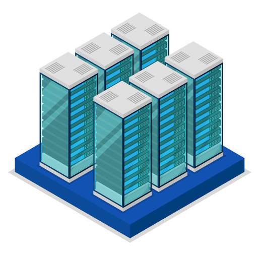
Server-to-Switch Data Center Links
Used for 10G/25G/100G optical uplinks between servers and top-of-rack switches in high-density data center deployments.

Building-to-Building Campus Backbone
Suitable for 1G/10G fiber links between office buildings, campus distribution rooms, and backbone aggregation points.

Access-to-Core Enterprise Uplinks
Designed for switch uplinks from access to aggregation or core layers in enterprise and campus network architectures.

Industrial Switching in Harsh Environments
Applied in industrial Ethernet, automation systems, and outdoor cabinets where wider temperature tolerance and stable fiber communication are required.
| Absolute Maximum Ratings | |||||||||
| Parameter | Symbol | Min. | Max. | Unit | |||||
| Storage temperature | TS | -40 | +85 | °C | |||||
| Supply voltage | VCC | -0.5 | 3.6 | V | |||||
| Note: Exceeding any one of these values may destroy the device permanently. | |||||||||
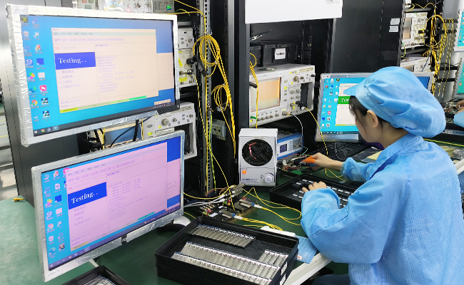
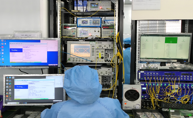
| Recommended Operating Conditions | |||||||||
| Parameter | Symbol | Min. | Typical | Max. | Unit | ||||
| Power supply voltage | Vcc | 3.15 | 3.3 | 3.45 | V | ||||
| Power supply current | Icc | - | - | 430 | mA | ||||
| Surge current | ISurge | - | - | +30 | mA | ||||
| Operating case temperature | Tc | Commercial | 0 | 70 | °C | ||||
| Industrial | -40 | 85 | °C | ||||||
| Baud rate | - | 0.6 | 10.3125 | 11.3 | GBaud | ||||
| Performance Specifications–Electrical | |||||||||
| Parameter | Symbol | Min. | Typ. | Max | Unit | Notes | |||
| Transmitter | |||||||||
| CML inputs(Differential) | Vin | 150 | - | 1200 | mVpp | AC coupled inputs | |||
| Input impedance (Differential) | Zin | 85 | 100 | 115 | ohms | Rin > 100 kohms @ DC | |||
| Tx_DISABLE input voltage - high | - | 2 | - | Vcc+0.3 | V | - | |||
| Tx_DISABLE input voltage - low | - | 0 | - | 0.8 | V | - | |||
| Tx_FAULT output voltage - high | - | 2 | - | Vcc+0.3 | V | Io = 400µA; Host Vcc | |||
| Tx_FAULT output voltage - low | - | 0 | - | 0.5 | V | Io = -4.0mA | |||
| Receiver | |||||||||
| CML outputs (Differential) | Vout | 350 | - | 700 | mVpp | AC coupled outputs | |||
| Output impedance (Differential) | Zout | 85 | 100 | 115 | ohms | - | |||
| Rx_LOS output voltage - high | - | 2 | - | Vcc+0.3 | V | lo = 400µA; Host Vcc | |||
| Rx_LOS output voltage - low | - | 0 | - | 0.8 | V | lo = -4.0mA | |||
| MOD_DEF ( 2:0 ) | VoH | 2.5 | - | - | V | With Serial ID | |||
| VoL | 0 | - | 0.5 | V | |||||
| Optical Characteristics-1270nm DFB & PIN/TIA | |||||||||
| Parameter | Symbol | Min. | Typical | Max. | Unit | ||||
| Power budget | - | 16 | - | - | dB | ||||
| Data rate | - | 0.6 | 10.3125 | 11.3 | Gbps | ||||
| Transmitter | |||||||||
| Centre wavelength | λC | 1260 | 1270 | 1280 | nm | ||||
| Spectral width (-20dB) | Δλ | - | - | 1 | nm | ||||
| Side mode suppression ratio | SMSR | 30 | - | - | dB | ||||
| Average output power | Pout, AVG | 1 | - | 5 | dBm | ||||
| Extinction ratio | ER | 3.5 | - | - | ms | ||||
| Average power of OFF transmitter | - | - | - | -30 | dBm | ||||
| Relative intensity noise | RIN | - | - | -128 | dB/Hz | ||||
| TX disable assert time | t_off | - | - | 10 | us | ||||
| Receiver | |||||||||
| Centre wavelength | λc | 1320 | - | 1340 | nm | ||||
| Sensitivity | PIN | - | - | -15 | dBm | ||||
| Receiver overload | PMAX | 0.5 | - | - | dBm | ||||
| LOS De-assert | LOSD | - | - | -18 | dBm | ||||
| LOS assert | LOSA | -30 | - | - | dBm | ||||
| Optical Characteristics-1330nm DFB & PIN/TIA | |||||||||
| Parameter | Symbol | Min. | Typical | Max. | Unit | ||||
| Power budget | - | 16 | - | - | dB | ||||
| Data rate | - | 0.6 | 10.3125 | 11.3 | Gbps | ||||
| Transmitter | |||||||||
| Centre wavelength | λC | 1320 | 1330 | 1340 | nm | ||||
| Spectral width (-20dB) | Δλ | - | - | 1 | nm | ||||
| Side mode suppression ratio | SMSR | 30 | - | - | dB | ||||
| Average output power | Pout, AVG | 1 | - | 5 | dBm | ||||
| Extinction ratio | ER | 3.5 | - | - | dB | ||||
| Average power of OFF transmitter | - | - | - | -30 | dBm | ||||
| Relative intensity noise | RIN | - | - | -128 | dB/Hz | ||||
| TX disable assert time | t_off | - | - | 10 | us | ||||
| Receiver | |||||||||
| Centre wavelength | λc | 1260 | - | 1280 | nm | ||||
| Sensitivity | PIN | - | - | -15 | dBm | ||||
| Receiver overload | PMAX | - | - | - | dBm | ||||
| LOS De-assert | LOSD | - | - | -18 | dBm | ||||
| LOS assert | LOSA | -30 | - | - | dBm | ||||
| SFP+ TRANSCEIVER ELECTRICAL PAD LAYOUT |
| PIN FUNCTION DEFINITIONS | |||||||||
| Pin | Name | Function | Plug Seq. | Notes | |||||
| 1 | VeeT | Transmitter ground | 1 | Note 5 | |||||
| 2 | TX Fault | Transmitter fault indication | 3 | Note 1 | |||||
| 3 | TX Disable | Transmitter disable | 3 | Note 2, module disables on high or open | |||||
| 4 | SDA | Module definition 2 | 3 | 2-Wire serial interface data line. | |||||
| 5 | SCL | Module definition 1 | 3 | 2-Wire serial interface clock. | |||||
| 6 | MOD-ABS | Module definition 0 | 3 | Note 3 | |||||
| 7 | RS0 | RX Rate select(LVTTL). | 3 | No function implement | |||||
| 8 | LOS | Loss of signal | 3 | Note 4 | |||||
| 9 | RS1 | TX Rate select(LVTTL). | 1 | No function implement | |||||
| 10 | VeeR | Receiver ground | 1 | Note 5 | |||||
| 11 | VeeR | Receiver ground | 1 | Note 5 | |||||
| 12 | RD- | Inv. received data out | 3 | Note 6 | |||||
| 13 | RD+ | Received data out | 3 | Note 6 | |||||
| 14 | VeeR | Receiver ground | 1 | Note 5 | |||||
| 15 | VccR | Receiver power | 2 | 3.3V ± 5%, Note 7 | |||||
| 16 | VccT | Transmitter power | 2 | 3.3V ± 5%, Note 7 | |||||
| 17 | VeeT | Transmitter ground | 1 | Note 5 | |||||
| 18 | TD+ | Transmit data in | 3 | Note 8 | |||||
| 19 | TD- | Inv. transmit data in | 3 | Note 8 | |||||
| 20 | VeeT | Transmitter ground | 1 | Note 5 | |||||
| Notes: 1) TX Fault is an open collector/drain output, which should be pulled up with a 4.7K – 10KΩ resistor on the host board. Pull up voltage between 2.0V and VccT/R+0.3V. When high, output indicates a laser fault of some kind. Low indicates normal operation. In the low state, the output will be pulled to < 0.8V. 2) TX disable is an input that is used to shut down the transmitter optical output. It is pulled up within the module with a 4.7K – 10 KΩ resistor. Its states are: Low (0 – 0.8V): Transmitter on (>0.8, < 2.0V): Undefined High (2.0 – 3.465V): Transmitter Disabled Open: Transmitter Disabled 3) Module Absent, connected to VeeT or VeeR in the module. 4) LOS (Loss of Signal) is an open collector/drain output, which should be pulled up with a 4.7K – 10KΩ resistor. Pull up voltage between 2.0V and VccT/R+0.3V. When high, this output indicates the received optical power is below the worst-case receiver sensitivity (as defined by the standard in use). Low indicates normal operation. In the low state, the output will be pulled to < 0.8V. 5) The module signal ground contacts, VeeR and VeeT, should be isolated from the module case. 6) RD-/+: These are the differential receiver outputs. They are AC coupled 100Ω differential lines which should be terminated with 100Ω (differential) at the user SERDES. The AC coupling is done inside the module and is thus not required on the host board. The voltage swing on these lines will be between 350 and 700 mV differential (175 –350 mV single ended) when properly terminated. 7) VccR and VccT are the receiver and transmitter power supplies. They are defined as 3.3V ±5% at the SFP+ connector pin. Maximum supply current is 430mA. Recommended host board power supply filtering is shown below. Inductors with DC resistance of less than 1 ohm should be used in order to maintain the required voltage at the SFP+ input pin with 3.3V supply voltage. When the recommended supply-filtering network is used, hot plugging of the SFP+ transceiver module will result in an inrush current of no more than 30mA greater than the steady state value. VccR and VccT may be internally connected within the SFP+ transceiver module. 8) TD-/+: These are the differential transmitter inputs. They are AC-coupled, differential lines with 100Ω differential termination inside the module. The AC coupling is done inside the module and is thus not required on the host board. The inputs will accept differential swings of 150 – 1200 mV (75 – 600mV single-ended). |
|||||||||

Performance Testing
Each module is tested before shipment to help ensure stable optical and electrical performance.

Compatibility Verification
Compatibility validation is available for major switch and router platforms.

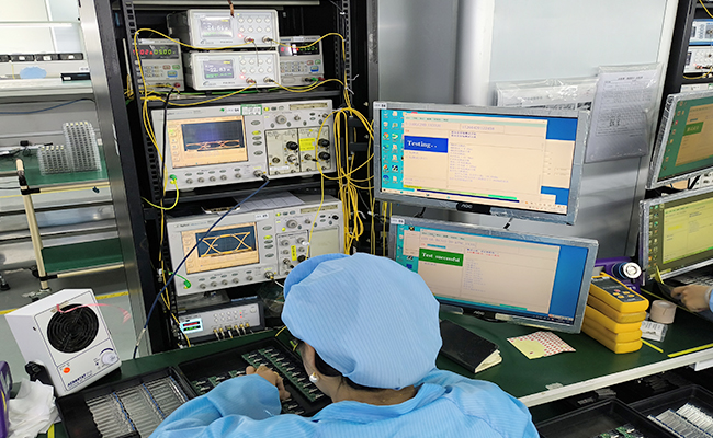
Reliability Screening
Selected products support aging, temperature cycle, and stability testing for demanding applications.

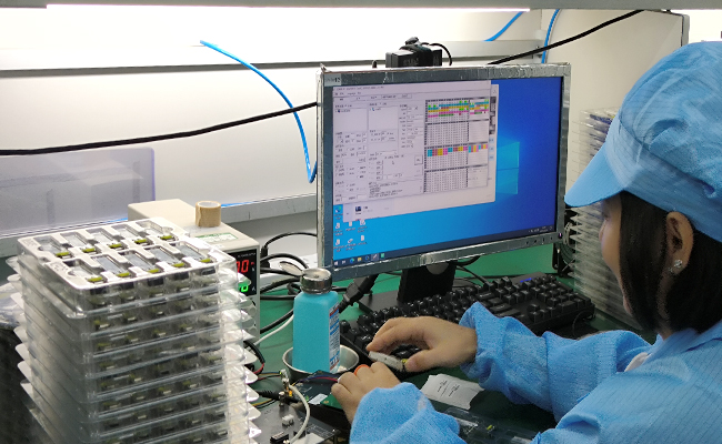
Traceable Quality Control
Inspection and production records support more consistent quality control and batch traceability.


