


40G CWDM4 QSFP+ LR4L Transceiver for 2km SMF Links, Duplex LC
QSFP+40-CW4-2(LR4L)-LCD
- Broad Multi-Brand Compatibility
- Flexible Customization Support
- Tested for Reliable Performance
- Fast Response & Delivery
- Professional Technical Support
The FC-LINK QSFP+ 40G CWDM4 2km LR4L LC DX transceiver modules are designed for 40 Gigabit per second links over single-mode fiber, compliant with the QSFP+ MSA and IEEE 802.3ba 40GBASE-LR4 standards. They support digital diagnostics via the I2C interface as outlined in the QSFP+ MSA. Additionally, these optical transceivers adhere to the RoHS Directive 2011/65/EU for environmental safety compliance.
| SPECIFICATIONS | |||
|---|---|---|---|
| Product Model | QSFP+40-CW4-2(LR4L)-LCD | Manufacturer Brand | FC-LINK |
| Package Type | QSFP+ | Optical Connector | LC Duplex |
| Max Data Rate | 40G | Channel Data Rate | 11.2Gbps |
| Effective Transmission Distance | 2km | ||
| Wavelength | 1271nm 1291nm 1311nm 1331nm | Operating Voltage | 3.3V |
| Fiber Type | SMF | Core Size | 9/125µm |
| Transmitter Type | 4 Lanes CWDM DFB | Receiver Type | PIN |
| TX Power | -7~+2.3dBm | Receiver Sensitivity | < -12dBm |
| Digital Diagnostic Monitoring(DDM) | YES | Receiver Overload | 2.3dBm |
| Power Consumption | ≤3.5W | Protocols | IEEE802.3ba 40GBASE-IR4 Standard |
| Operating temperature(Commercial) | 0℃~+70℃ | Storage Temperature(Commercial) | -40℃~+85℃ |

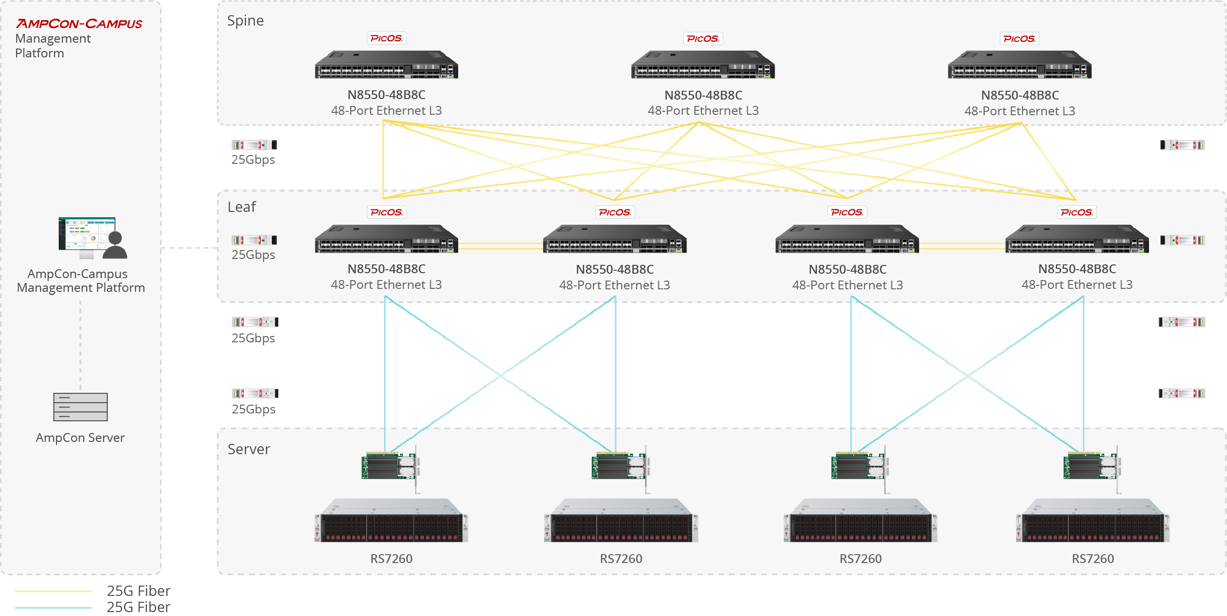
Server-to-Switch Data Center Links
Used for 10G/25G/100G optical uplinks between servers and top-of-rack switches in high-density data center deployments.

Building-to-Building Campus Backbone
Suitable for 1G/10G fiber links between office buildings, campus distribution rooms, and backbone aggregation points.

Access-to-Core Enterprise Uplinks
Designed for switch uplinks from access to aggregation or core layers in enterprise and campus network architectures.

Industrial Switching in Harsh Environments
Applied in industrial Ethernet, automation systems, and outdoor cabinets where wider temperature tolerance and stable fiber communication are required.
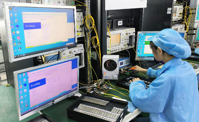
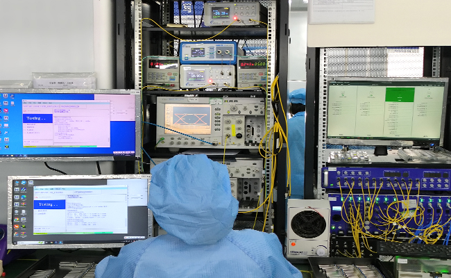
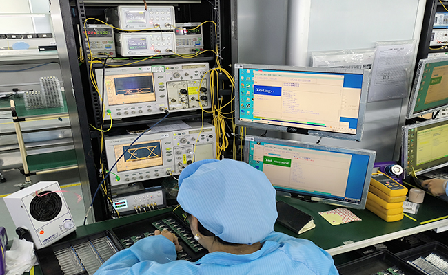
| General Specifications-1 | |||||||||
| Parameter | Value | Unit | Notes | ||||||
| Module Form Factor | QSFP+ | - | - | ||||||
| Number of Lanes | 4 Tx and 4 | - | - | ||||||
| Maximum Aggregate Data Rate | 41.2 | Gb/s | - | ||||||
| Maximum Data Rate per Lane | 10.3 | Gb/s | Higher bit rates may be supported. Please contact FS. | ||||||
| Protocols Supported | Typical applications include 40G Ethernet, Infiniband Fibre Channel, SATA/SAS3 | - | - | ||||||
| Electrical Interface and Pin-out | 38-pin edge connector | - | Pin-out as defined by the QSFP+ MSA | ||||||
| Maximum Power Consumption | 3.5 | - | - | ||||||
| Management Interface | Serial, I2C-based, 400 kHz maximum frequency | As defined by the QSFP+ MSA | |||||||
| General Specifications-2 | |||||||||
| Data Rate Specifications | Symbol | Min | Typ. | Max | Units | Ref. | |||
| Bit Rate per Lane | BR | - | - | 10313 | Mb/sec | 1 | |||
| Bit Error Ratio | BER | - | - | 10-12 | - | 2 | |||
| Link distance on SMF-28 | d | - | - | 2 | kilometers | 3 | |||
| Notes: 1.Compliant with 40GBASE-LR4 and XLPPI per IEE 802.3ba. Compatible with 1/10 Gigabit Ethernet and 1/2/4/8/10G Fibre Channel. 2.Tested with a PRBS 231-1 test pattern. 3.Per 40GBASE-LR4, IEEE 802.3ba. |
|||||||||
| Absolute Maximum Ratings | |||||||||
| Parameter | Symbol | Min | Typ. | Max | Unit | Ref. | |||
| Maximum supply voltage | Vcc1, VccTx, VccRx | -0.5 | - | 3.6 | V | - | |||
| Supply voltage | Ts | -40 | - | +85 | °C | - | |||
| Case operating temperature | Top | +15 | - | +60 | °C | - | |||
| Relative humidity | RH | 0 | - | 85 | % | 1 | |||
| Damage threshold, per lane | DT | 3.4 | - | - | dBm | - | |||
| Note: 1.Non-condensing. |
|||||||||
| Electrical Characteristics | |||||||||
| Parameter | Symbol | Min | Typ. | Max | Unit | Ref. | |||
| Supply voltage | Vcc1, VccTx, VccRx | 3.1 | - | 3.47 | V | - | |||
| Supply current | Icc | - | - | 1.13 | A | - | |||
| Transmit turn-on time | - | - | - | 2000 | ms | 1 | |||
| Transmitter (per lane) | |||||||||
| Single ended input voltage tolerance | VinT | -0.3 | - | 4.0 | V | - | |||
| Differential data input swing | Vin,pp | 120 | - | 1200 | mVpp | 2 | |||
| Differential input threshold | - | - | 50 | - | mV | - | |||
| AC common mode input voltage tolerance (RMS) | - | 15 | - | - | mV | - | |||
| J2 jitter tolerancez | Jt2 | 0.17 | - | - | UI | - | |||
| J9 jitter tolerance | Jt9 | 0.29 | - | - | UI | - | |||
| Data dependent pulse width shrinkage | DDPWS | 0.07 | - | - | UI | - | |||
| Eye mask colordinates {X1, X2 ,Y1, Y2} |
- | - | 0.11, 0.31 95, 350 |
- | UI mV |
4 | |||
| Receiver (per lane) | |||||||||
| Single-ended output voltage | - | -0.3 | - | 4.0 | V | - | |||
| Differential data output swing | Vout,pp | 200 | - | 400 | mVpp | 5,6 | |||
| 300 | - | 600 | |||||||
| 400 | 550 | 800 | |||||||
| 600 | - | 1200 | |||||||
| AC common mode output voltage (RMS) | - | - | - | 7.5 | mV | - | |||
| Termination mismatch at 1 MHx | - | - | - | 5 | % | - | |||
| Differential output return loss | - | Per IEEE P802.3ba,Section 86A.4.2.1 | dB | 3 | |||||
| Common mode output return loss | - | Per IEEE P802.3ba,Section 86A.4.2.2 | dB | 3 | |||||
| Output transition time, 20% to 80% | - | 28 | - | - | ps | - | |||
| J2 jitter output | Jo2 | - | - | 0.42 | UI | - | |||
| J9 jitter output | Jo9 | - | - | 0.65 | UI | - | |||
| Eye mask coordinates #1 {X1, X2, Y1, Y2} |
- | - | 0.29, 0.5 150, 425 |
- | UI mV |
4 | |||
| Power supply ripple tolerance | PSR | 50 | - | - | mVpp | - | |||
| Notes: 1.From power-on and end of any fault conditions. 2.After internal AC coupling. Self-biasing 100Ω differential input. 3.10 MHz to 11.1 GHz range 4.Hit ratio = 5 x 10E-5. 5.AC coupled with 100Ωdifferential output impedance. 6.Output voltage is settable in 4 discrete steps via the I2C. Default is 400-800 mV. |
|||||||||
| Optical Characteristics | |||||||||
| Parameter | Symbol | Min | Typ. | Max | Unit | Ref. | |||
| Transmitter (per lane) | |||||||||
| Signaling speed per lane | - | - | - | 10.3125 | GBd | 1 | |||
| Lane center wavelengths (range) | - | 1264.5-1277.5 1284.5-1297.5 1304.5-1317.5 1324.5-1337.5 |
nm | - | |||||
| Total average launch power | Pout | - | - | 8.3 | dBm | - | |||
| Average launch power per lane | TXPx | -7.0 | - | 2.3 | dBm | - | |||
| Transmit OMA per lane | TxOMA | -4.0 | - | 3.5 | dBm | 2 | |||
| Optical extinction ratio | ER | 3.5 | - | - | dB | - | |||
| Sidemode suppression ratio | SSRmin | 30 | - | - | dB | - | |||
| Average launch power of OFF transmitter, per lane | - | - | -30 | dBm | |||||
| Relative intensity tolerance | RIN | - | - | -128 | dB/Hz | 3 | |||
| Optical return loss tolerance | - | - | - | 20 | - | - | |||
| Transmitter reflectance | - | - | - | -12 | dB | - | |||
| Transmitter eye mask definition {X1, X2, X3, Y1, Y2, Y3} |
- | (0.25, 0.4, 0.45, 0.25, 0.28, 0.4) |
- | - | - | - | |||
| Parameter | Symbol | Min | Typ. | Max | Unit | Ref. | |||
| Receiver (per lane) | |||||||||
| Signaling speed per lane | - | - | - | 10.3125 | GBd | 4 | |||
| Lane center wavelengths (range) | - | 1264.5-1277.5 1284.5-1297.5 1304.5-1317.5 1324.5-1337.5 |
nm | - | |||||
| Receive power (OMA) per lane | RxOMA | - | 3.5 | dBm | |||||
| Average receive power per lane | RXPx | -11.5 | - | 2.3 | dBm | 5 | |||
| Receiver sensitivity (OMA) per lane | Rxsens | - | - | -11.5 | dBm | - | |||
| Stressed receiver sensitivity (OMA) per lane | SRS | - | - | -9.6 | dBm | - | |||
| Damage threshold per lane | PMAX | - | - | 3.4 | dBm | - | |||
| Return loss | RL | - | - | -26 | dB | - | |||
| Vertical eye closure penalty, per lane | - | - | - | 1.9 | dB | - | |||
| Receive electrical 3dB upper cutoff frequency, per lane | - | - | - | 12.3 | GHz | - | |||
| LOS De-assert | LOSD | - | - | -15 | dBm | - | |||
| LOS assert | LOSA | -28 | - | - | dBm | - | |||
| LOS hysteresis | - | - | 1 | - | dB | - | |||
| Notes: 1.Transmitter consists of 4 lasers operating at 10.3Gb/s each. 2.Minimum value is informative. 3.RIN is scaled by 10*log(10/4) to maintain SNR outside of transmitter. 4.Receiver consists of 4 photodetectors operating at 10.3Gb/s each. 5.Minimum value is informative, equals min TxOMA with infinite ER and max channel insertion loss. |
|||||||||
| Pin Description |
QSFP+ MSA-compliant 38-pin connector
| Pin | Symbol | Name/Description | Notes | ||||||
| 1 | GND | Ground | 1 | ||||||
| 2 | Tx2n | Transmitter Inverted Data Input | - | ||||||
| 3 | Tx2p | Transmitter Non-Inverted Data Input | - | ||||||
| 4 | GND | Ground | 1 | ||||||
| 5 | Tx4n | Transmitter Inverted Data Input | - | ||||||
| 6 | Tx4p | Transmitter Non-Inverted Data Input | - | ||||||
| 7 | GND | Ground | 1 | ||||||
| 8 | ModSelL | Module Select | - | ||||||
| 9 | ResetL | Module Reset | - | ||||||
| 10 | Vcc Rx | +3.3V Power Supply Receiver | - | ||||||
| 11 | SCL | 2-wire Serial Interface Clock | - | ||||||
| 12 | SDA | 2-wire Serial Interface Data | - | ||||||
| 13 | GND | Ground | 1 | ||||||
| 14 | Rx3p | Receiver Non-Inverted Data Output | - | ||||||
| 15 | Rx3n | Receiver Inverted Data Output | - | ||||||
| 16 | GND | Ground | 1 | ||||||
| 17 | Rx1p | Receiver Non-Inverted Data Output | - | ||||||
| 18 | Rx1n | Receiver Inverted Data Output | - | ||||||
| 19 | GND | Ground | 1 | ||||||
| 20 | GND | Ground | 1 | ||||||
| 21 | Rx2n | Receiver Inverted Data Output | - | ||||||
| 22 | Rx2p | Receiver Non-Inverted Data Output | - | ||||||
| 23 | GND | Ground | 1 | ||||||
| 24 | Rx4n | Receiver Inverted Data Output | - | ||||||
| 25 | Rx4p | Receiver Non-Inverted Data Output | - | ||||||
| 26 | GND | Ground | 1 | ||||||
| 27 | ModPrsL | Module Present | - | ||||||
| 28 | IntL | Interrupt | - | ||||||
| 29 | Vcc Tx | +3.3V Power Supply Transmitter | - | ||||||
| 30 | Vcc1 | +3.3V Power Supply | - | ||||||
| 31 | LPMode | Low Power Mode | - | ||||||
| 32 | GND | Ground | - | ||||||
| 33 | Tx3p | Transmitter Non-Inverted Data Input | 33 | ||||||
| 34 | Tx3n | Transmitter Inverted Data Input | - | ||||||
| 35 | GND | Ground | 1 | ||||||
| 36 | Tx1p | Transmitter Non-Inverted Data Input | - | ||||||
| 37 | Tx1n | Transmitter Inverted Data Input | - | ||||||
| 38 | GND | Ground | 1 | ||||||
| Note: Circuit ground is internally isolated from chassis ground. |
|||||||||

Performance Testing
Each module is tested before shipment to help ensure stable optical and electrical performance.

Compatibility Verification
Compatibility validation is available for major switch and router platforms.

Reliability Screening
Selected products support aging, temperature cycle, and stability testing for demanding applications.

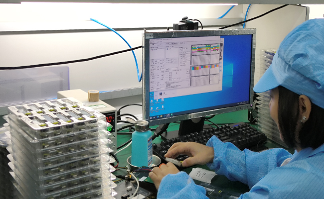
Traceable Quality Control
Inspection and production records support more consistent quality control and batch traceability.


