10G CWDM SFP+ ER Transceiver for SMF Links, 1270nm to 1450nm Duplex LC

SFP+10-CW1214-ER-LCD

  • Broad Multi-Brand Compatibility
  • Flexible Customization Support
  • Tested for Reliable Performance
  • Fast Response & Delivery
  • Professional Technical Support

The FC-LINK SFP+ 10G CWDM (1270-1450nm) ER LC DX series optical transceiver is designed for high-performance fiber communication applications, such as 10G Ethernet (10GBASE-ZR/ZW), and is fully compliant with the SFP+ MSA SFF-8431 specification. This module is optimized for single-mode fiber and operates across CWDM wavelengths, with ten available center wavelengths ranging from 1270nm to 1450nm, spaced 20nm apart. It offers a guaranteed optical link budget of 23dB. The module features an SFP+ connector for hot-plug capability and requires only a single 3.3V power supply. The optical output can be disabled via an LVTTL logic high-level input (TX_DIS), and a Loss of Signal (RX_LOS) output is provided to indicate the absence of an optical signal at the receiver.

SPECIFICATIONS
Product ModelSFP+10-CW1214-ER-LCDManufacturer BrandFC-LINK
Package TypeSFP+Optical ConnectorDuplex LC
Max Data Rate11.3GbpsChannel Data Rate10.138Gb/s
Power Budget23dB
Wavelength1270nm to 1450nmOperating Voltage3.3V
Fiber TypeSMFCore Size9/125µm
Transmitter TypeCWDM DFBReceiver TypeIDP
TX Power2~5dBmReceiver Sensitivity-21dBm
Digital Diagnostic Monitoring(DDM)YESReceiver Overload-6dBm
Power Consumption<1.5WProtocolsSFF-8431
SFF-8472
Operating Temperature(Commercial)0℃~+70℃Storage Temperature(Commercial)-40℃~+85℃
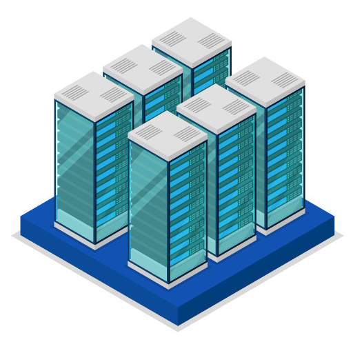
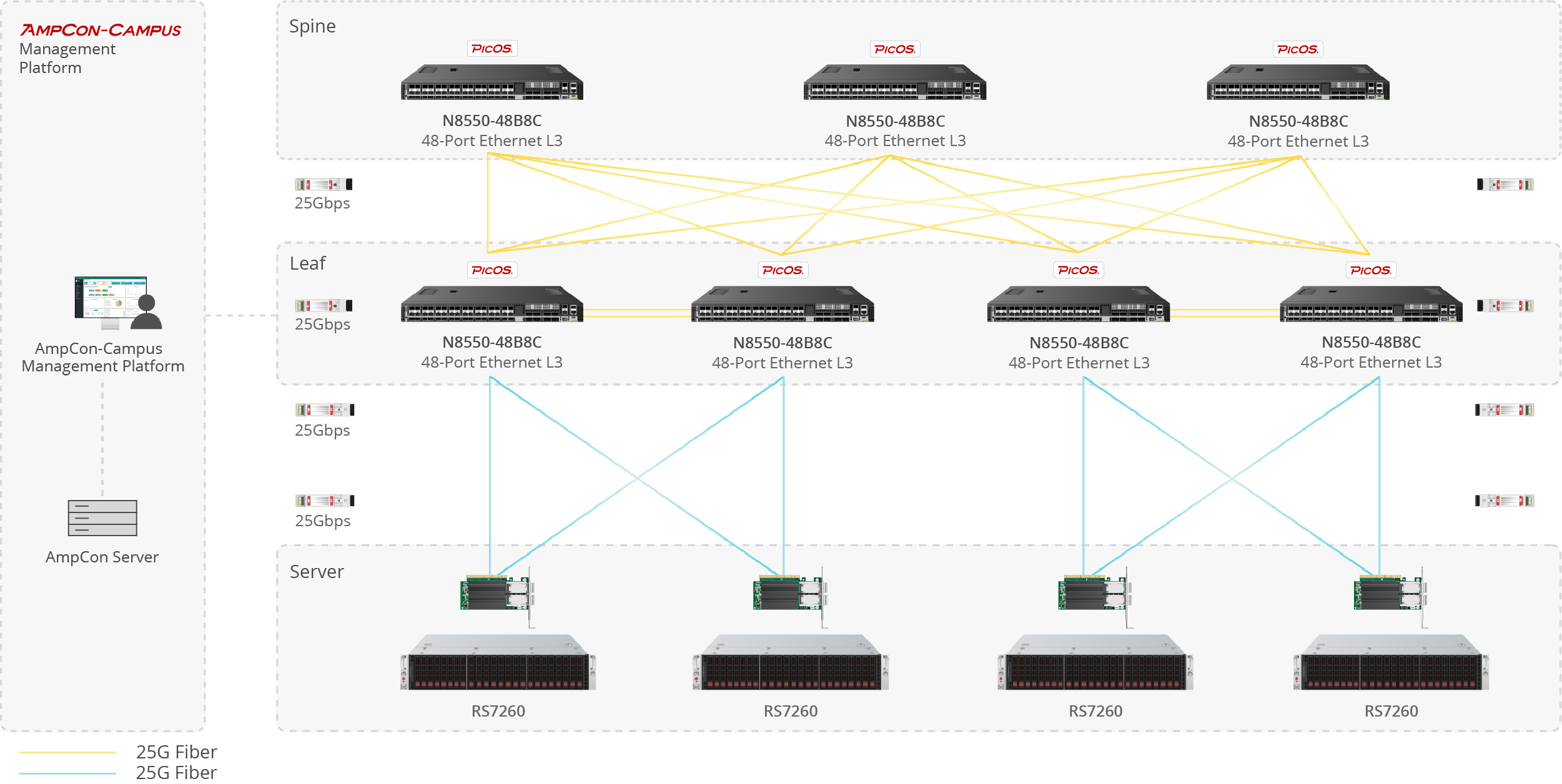
Server-to-Switch Data Center Links

Used for 10G/25G/100G optical uplinks between servers and top-of-rack switches in high-density data center deployments.

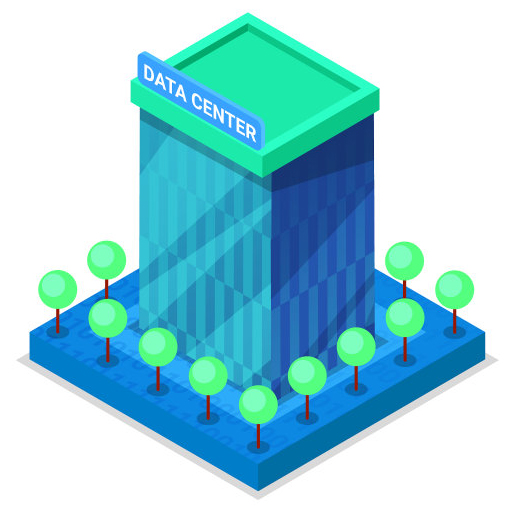
Building-to-Building Campus Backbone

Suitable for 1G/10G fiber links between office buildings, campus distribution rooms, and backbone aggregation points.

Access-to-Core Enterprise Uplinks

Designed for switch uplinks from access to aggregation or core layers in enterprise and campus network architectures.

Industrial Switching in Harsh Environments

Applied in industrial Ethernet, automation systems, and outdoor cabinets where wider temperature tolerance and stable fiber communication are required.
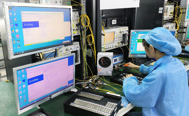
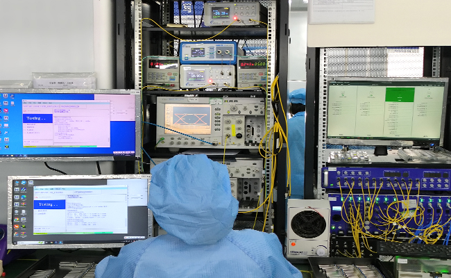

网络拓扑展示模块
1
1
1

Compatible Brands

Customization Options

Vendor Coding
Private Label
Custom Part Number
Packaging Design
Temperature Grade Selection
CWDM* Wavelength
Band Nomenclature Wavelength(nm)
Min. Typ. Max.
O-band original A 1264  1270  1277.5 
B 1284  1290  1297.5 
C 1304  1310  1317.5 
D 1324  1330  1337.5 
O-band original E 1344  1350  1357.5 
E-band extended F 1364  1370  1377.5 
G 1384  1390  1397.5 
H 1404  1410  1417.5 
I 1424  1430  1437.5 
J 1444       1450  1457.5 
CWDM*: 10 Wavelengths from 1270nm to 1330nm, each step 20nm.

Absolute Maximum Ratings
Parameter Symbol Min. Typical Max. Unit
Maximum supply voltage 1 Vcc -0.5  - 4.0  V
Storage temperature Ts -40  - 85  °C

Recommended Operating Conditions
Parameter Symbol Min. Typical Max. Unit
Case operating temperature TC -5 - +70  °C
Supply voltage Vcc 3.15  3.3  3.45  V
Supply current Icc - - 430  mA
Data rate - 0.614 - 11.3  Gbps

Electrical Characteristics
Parameter Symbol Min. Typ. Max Unit Notes
Transmitter
CML inputs(Differential) Vin 180 - 1000 mVpp 1
Input impedance (Differential) Zin 85 100 115 ohms -
Tx_DISABLE input voltage - high - 2 - Vcc+0.3 V -
Tx_DISABLE input voltage - low - 0 - 0.8 V -
Tx_FAULT output voltage - high - 2 - Vcc+0.3 V -
Tx_FAULT output voltage - low - 0 - 0.8 V -
Receiver
CML Outputs (Differential) Vout 350 - 700 mVpp 1
Output impedance (Differential) Zout 85 100 115 ohms -
Rx_LOS output voltage - high - 2 - Vcc+0.3 V -
Rx_LOS output voltage - low - 0 - 0.8 V -
MOD_DEF ( 0:2 ) VoH 2.5 - - V 2
VoL 0 - 0.5 V
Notes:
1. After internal AC coupling.
2. Reference the SFF-8472 MSA.

Optical Characteristics
Parameter Symbol Min. Typical Max. Unit Notes
Transmitter
Output opt. pwr: 9/125 SMF Pout 2 - +5  dBm 1
Optical extinction ratio ER 3.5 - - dB -
Optical wavelength λc λc–6 λc λc+7.5 nm 2
-20dB spectrum width Δλ - - 1 nm -
Side mode suppression ratio SMSR 30 - - dB -
Average launch power of OFF transmitter POFF - - -30 dBm -
TX jitter TXj Per 802.3ae requirements - -
Relative intensity noise RIN - - -128 dB/Hz -
Receiver
Receiver sensitivity @ 10.3125Gb/s Pmin - - 21 dBm 3
Maximum input power Pmax -6 - - dBm -
Optical center wavelength λ 1260 - 1460 nm -
Receiver reflectance Rrf - - -12 dB -
LOS de-assert LOSD - - -23 dBm -
LOS assert LOSA -35 - - dBm -
LOS hysteresis - 1 - - dB -
*Notes:
1. Output power is coupled into a 9/125μm SMF.
2. ITU-T G.694.2 CWDM wavelength from 1270nm to 1450nm, each step 20nm.
3. Average received power; BER less than 1E-12 and PRBS 231-1 test pattern.

SFP+ TRANSCEIVER ELECTRICAL PAD LAYOUT

PIN FUNCTION DEFINITIONS
Pin Name Function Plug Seq. Notes
1 VeeT Transmitter ground Note 5
2 TX Fault Transmitter fault indication Note 1
3 TX Disable Transmitter disable Note 2, module disables on high or open
4 SDA Module definition 2 2-Wire serial interface data line.
5 SCL Module definition 1 2-Wire serial Interface clock.
6 MOD-ABS Module definition 0 Note 3
7 RS0 RX rate select(LVTTL). No function implement
8 LOS Loss of signal Note 4
9 RS1 TX rate select(LVTTL). No function implement
10 VeeR Receiver ground Note 5
11 VeeR Receiver ground Note 5
12 RD- Inv. received data out 3 Note 6
13 RD+ Received data out 3 Note 6
14 VeeR Receiver ground Note 5
15 VccR Receiver power 3.3V ± 5%, Note 7
16 VccT Transmitter power 3.3V ± 5%, Note 7
17 VeeT Transmitter ground Note 5
18 TD+ Transmit data in Note 8
19 TD- Inv. transmit data in Note 8
20 VeeT Transmitter ground Note 5
Notes:
1) TX Fault is an open collector/drain output, which should be pulled up with a 4.7K – 10KΩ resistor on the host board. Pull up voltage between 2.0V and VccT/R+0.3V. When high, output  indicates a laser fault of some kind. Low indicates normal operation. In the low state, the output will be pulled to < 0.8V.

2) TX disable is an input that is used to shut down the transmitter optical output. It is pulled up within the module with a 4.7K~10 K Ω resistor. Its states are:
Low (0 – 0.8V): Transmitter on
(>0.8, < 2.0V): Undefined
High (2.0 – 3.465V): Transmitter Disabled
Open: Transmitter Disabled

3) Module Absent, connected to VeeT or VeeR in the module.

4) LOS (Loss of Signal) is an open collector/drain output, which should be pulled up with a 4.7K –10KΩ resistor on host board. Pull up voltage between 2.0V and VccT/R+0.3V. When high, this output indicates the received optical power is below the worst-case receiver sensitivity (as defined by the standard in use). Low indicates normal operation. In the low state, the output will be pulled to < 0.8V.

5) The module signal ground contacts, VeeR and VeeT, should be isolated from the module case.

6) RD-/+: These are the differential receiver outputs. They are AC coupled 100Ω differential lines which should be terminated with 100Ω (differential) at the user SERDES. The AC coupling is done inside the module and is thus not required on the host board. The voltage swing on these lines will be between 370 and 700 Mv differential (185–350Mv single ended) when properly terminated.

7) VccR and VccT are the receiver and transmitter power supplies. They are defined as 3.3V ±5% at the SFP+ connector pin. Maximum supply current is 300mA. Recommended host board power supply filtering is shown below. Inductors with DC resistance of less than 1 ohm should be used in order to maintain the required voltage at the SFP+ input pin with 3.3V supply voltage. When the recommended supply-filtering network is used, hot plugging of the SFP+ transceiver module will result in an inrush current of no more than 30Ma greater than the steady state value. VccR and VccT may be internally connected within the SFP+ transceiver module.

8) TD-/+: These are the differential transmitter inputs. They are AC-coupled, differential lines with 100Ω differential termination inside the module. The AC coupling is done inside the module and is thus not required on the host board.

Performance Testing

Each module is tested before shipment to help ensure stable optical and electrical performance.

Compatibility Verification

Compatibility validation is available for major switch and router platforms.

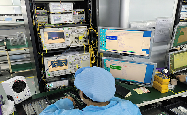
Reliability Screening

Selected products support aging, temperature cycle, and stability testing for demanding applications.

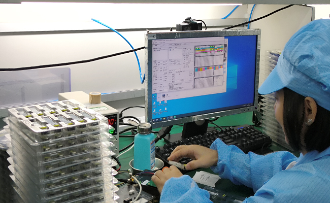
Traceable Quality Control

Inspection and production records support more consistent quality control and batch traceability.

光模块产品详情订购信息---SFP+(CWDM/DWDM)