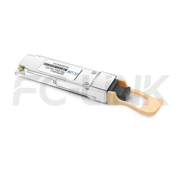
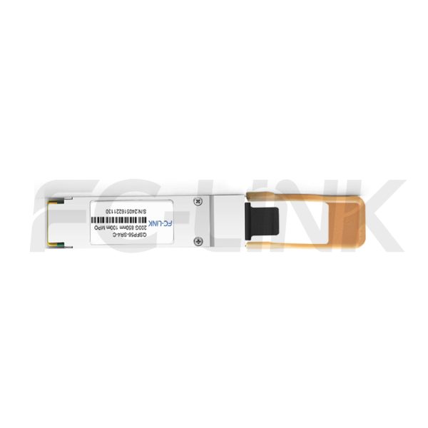
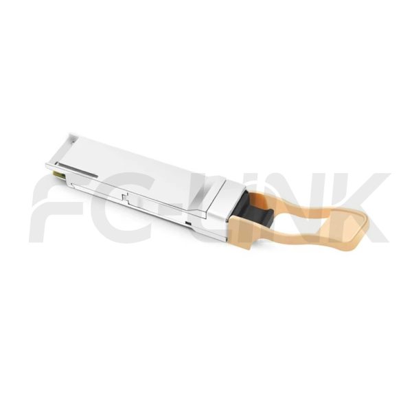
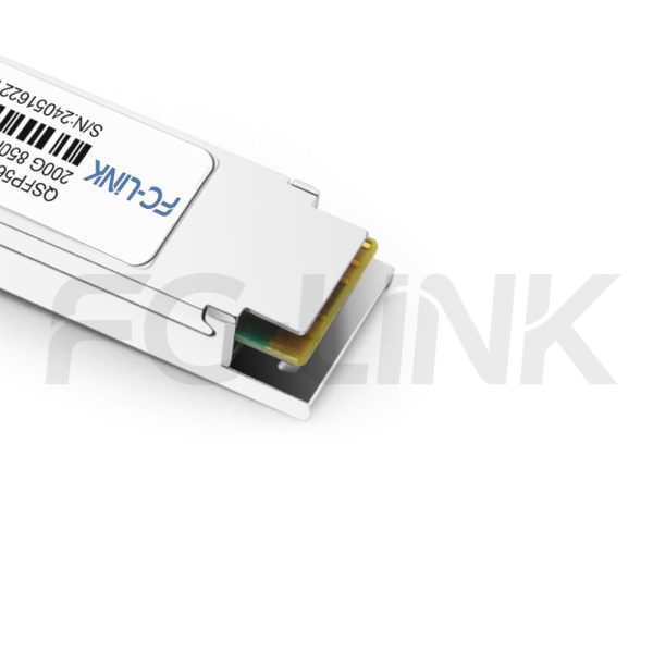
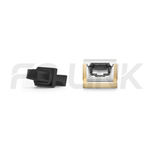
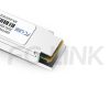
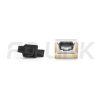


Generic Compatible 200GBASE-SR4 QSFP56 850nm 100m DOM MPO8/12 MMF Optical Transceiver Module
QSFP56-200-85-01(SR4)-MPO8/12
- Broad Multi-Brand Compatibility
- Flexible Customization Support
- Tested for Reliable Performance
- Fast Response & Delivery
- Professional Technical Support
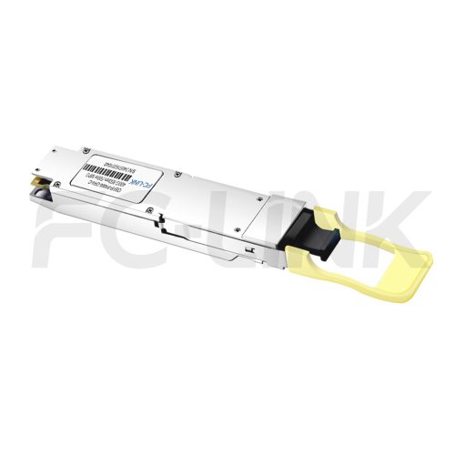
The FC-LINK QSFP56 200G 850nm 100m SR4 MPO8/12 Transceiver is a high-performance, pluggable fiber-optic module designed for 200Gbps short-range (SR) applications. It features four channels, each operating at 53.125Gbps, and supports data transmission distances of up to 70 meters over OM3 fiber and 100 meters over OM4 fiber. The transceiver employs an MPO receptacle for its optical interface and utilizes a 38-contact edge-type connector for its electrical interface. Optimized for multimode fiber systems, it operates at a nominal wavelength of 850nm, making it ideal for efficient and reliable short-range data communication and interconnect solutions.

| SPECIFICATIONS | |||
|---|---|---|---|
| Product Model | QSFP56-200-85-01(SR4)-MPO8/12 | Manufacturer brand | FC-LINK |
| Package Type | QSFP56 | Optical connector | MPO 8C/12C |
| Max Data Rate | 200Gbps | Channel Data Rate | 53.125Gbps |
| Effective transmission distance(OM3) | 70m | Effective transmission distance(OM4) | 100m |
| Wavelength | 850nm | Operating voltage | 3.3V |
| Fiber Type | MMF | Core Size | 50/125 |
| Transmitter Type | VCSEL | Receiver Type | PIN |
| TX Power | -8.4~4.0dBm | Receiver Sensitivity | -6.5dBm |
| Digital Optical Monitoring(DOM) | YES | Receiver Overload | 4dBm |
| Power Consumption | TSOM4-NAALA1C-01<5.5W TSOM4-NAALA1C-02<6W | Protocols | 200G BASE-SR4 Ethernet |
| Operating temperature(Commercial) | 0℃~+70℃ | Storage Temperature(Commercial) | -40℃~+85℃ |

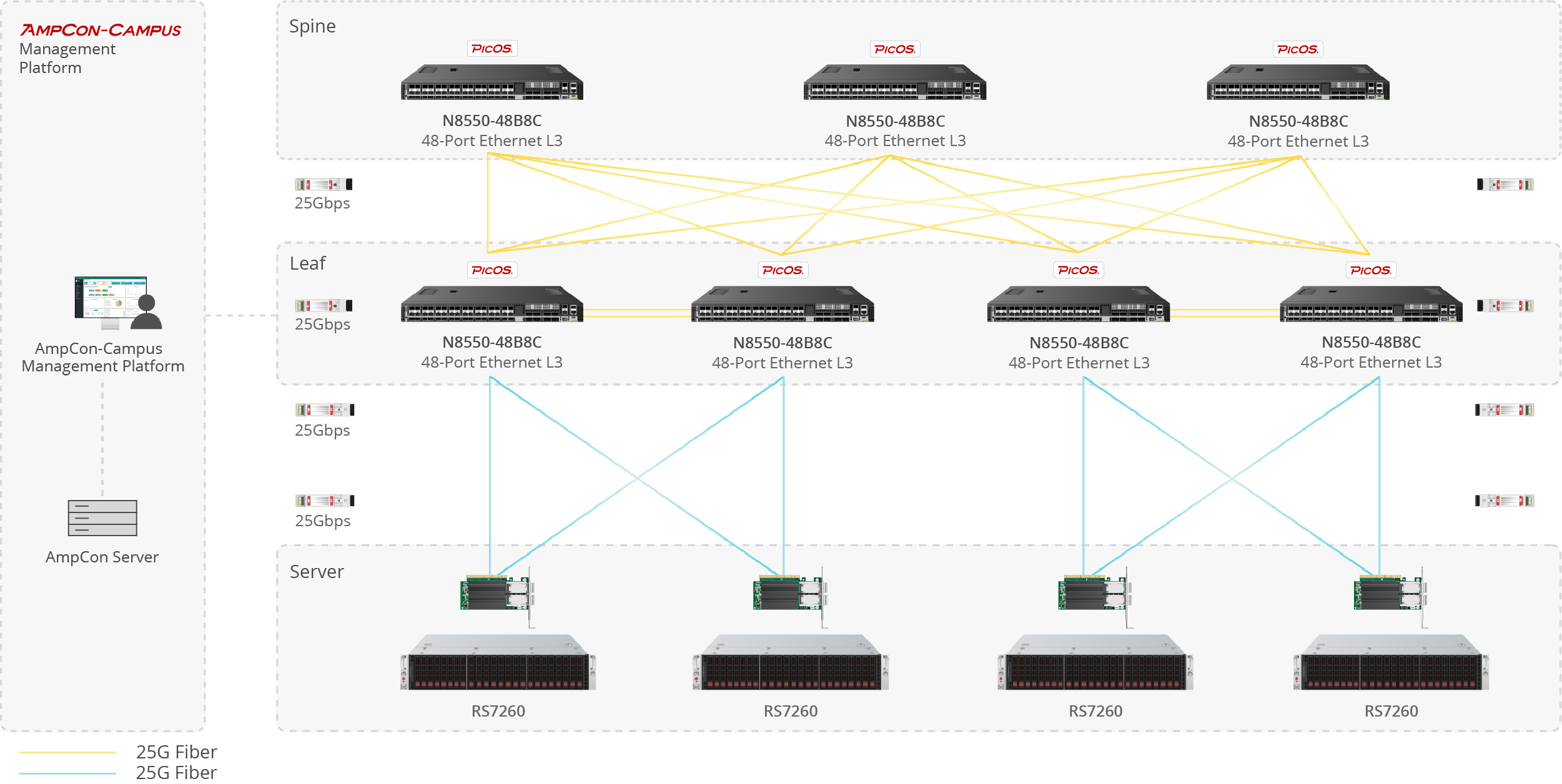
Server-to-Switch Data Center Links
Used for 10G/25G/100G optical uplinks between servers and top-of-rack switches in high-density data center deployments.

Building-to-Building Campus Backbone
Suitable for 1G/10G fiber links between office buildings, campus distribution rooms, and backbone aggregation points.

Access-to-Core Enterprise Uplinks
Designed for switch uplinks from access to aggregation or core layers in enterprise and campus network architectures.

Industrial Switching in Harsh Environments
Applied in industrial Ethernet, automation systems, and outdoor cabinets where wider temperature tolerance and stable fiber communication are required.
| Absolute Maximum Ratings | |||||||||
| Parameter | Symbol | Min. | Max. | Unit | |||||
| Power supply voltage | VCC | -0.5 | 3.6 | V | |||||
| Storage temperature | TC | -40 | 85 | ℃ | |||||
| Relative humidity | RH | 5 | 85 | % | |||||
| These values represent the damage threshold of the module.Stress in excess of any of the individual absolute maximum ratingscan cause immediate catastrophic damage to the module even if all other parameters are within recommended operating conditions. | |||||||||
| Recommended Operating Environment | |||||||||
| Parameter | Symbol | Min | Typical | Max | Unit | ||||
| Power supply voltage | VCC | 3.15 | 3.3 | 3.45 | V | ||||
| Operating case temperature | Tca | 0 | - | 70 | ℃ | ||||
| Recommended operating environment specifies parameters for which the electrical and optical characteristics hold unless otherwise noted. | |||||||||
| Electrical Characteristics | |||||||||
| Parameter | Symbol | Min | Typical | Max | Unit | Notes | |||
| Data rate per lane | DR | - | 53.125 | - | Gbps | - | |||
| Transmitter | |||||||||
| Single ended output voltage tolerance | - | -0.3 | - | 4 | V | - | |||
| Common mode voltage tolerance | - | 15 | - | - | mV | - | |||
| Input differential impedance | Rin | - | 100 | - | Ω | - | |||
| Differential input voltage swing | Vin | 300 | - | 1100 | mV | - | |||
| Tx fault | VoL | -0.3 | - | 0.4 | V | At 0.7mA | |||
| Receiver | |||||||||
| Single ended output voltage tolerance | - | -0.3 | - | 4 | V | - | |||
| Differential output swing | Vout | 300 | - | 900 | mV | - | |||
| Output differential impedance | Rout | - | 100 | - | Ω | - | |||
| The following electrical characteristics are defined over the recommended operating environment unless otherwise specified. | |||||||||
| Optical Characteristics | |||||||||
| Parameter | Symbol | Min | Typical | Max | Unit | Notes | |||
| Transmitter | |||||||||
| Center wavelength | λ | 820 | 850 | 880 | nm | - | |||
| RMS spectral width | Pm | - | - | 0.6 | nm | 1 | |||
| Average optical power | Po | -6.5 | - | 4 | dBm | 2 | |||
| Extinction ratio | ER | 3 | - | - | dBm | - | |||
| Optical modulation amplitude | OMA | -4.5 | - | 3 | dB | - | |||
| Transmitter and dispersion eye closure | TDECQ | - | - | 4.5 | dB | - | |||
| Optical return loss tolerance | ORL | - | - | 12 | dB | - | |||
| Receiver | |||||||||
| Center wavelength | λ | 820 | - | 880 | nm | - | |||
| Average receive power,each lane | - | -8.4 | - | 4 | dBm | - | |||
| Receive power(OMAouter),each lane | - | - | - | 4 | dBm | - | |||
| Receiver sensitivity(OMAAut) | Psens | - | - | -6.5 | dBm | 3 | |||
| LOS asserted | Lsa | -30 | - | - | dBm | - | |||
| LOS De-asserted | Lda | - | - | -10 | dBm | - | |||
| LOS hysteresis | Lh | 0.5 | - | - | dB | - | |||
| Note: [1]Trade-offs are available between spectral width,center wavelength and minimum OMA. [2]The optical power is launched into MMF [3]BER=2.4E-4;PRBS31Q@26.5625GBd.Pre-FEC | |||||||||
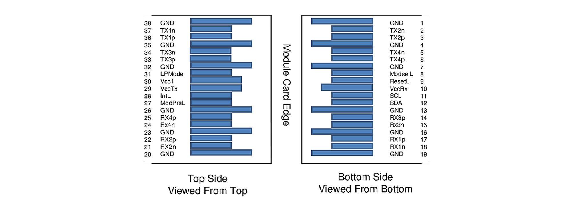
| QSFP56 Transceiver Electrical Pad Layout |
| Pin Definition | |||||||||
| Pin | Symbol | Name/Description | |||||||
| 1 | GND | Ground | |||||||
| 2 | Tx2n | Transmitter inverted data input | |||||||
| 3 | Tx2p | Transmitter non-inverted data input | |||||||
| 4 | GND | Ground | |||||||
| 5 | Tx4n | Transmitter inverted data input | |||||||
| 6 | Tx4p | Transmitter non-inverted data input | |||||||
| 7 | GND | Ground | |||||||
| 8 | ModSelL | Module select | |||||||
| 9 | ResetL | Module reset | |||||||
| 10 | VCCRx | +3.3V power supply receiver | |||||||
| 11 | SCL | 2-wire serial interface clock | |||||||
| 12 | SDA | 2-wire serial interface data | |||||||
| 13 | GND | Ground | |||||||
| 14 | Rx3p | Receiver non-inverted data output | |||||||
| 15 | Rx3n | Receiver inverted data output | |||||||
| 16 | GND | Ground | |||||||
| 17 | Rxlp | Receiver non-inverted data output | |||||||
| 18 | Rx1n | Receiver inverted data output | |||||||
| 19 | GND | Ground | |||||||
| 20 | GND | Ground | |||||||
| 21 | Rx2n | Receiver inverted data output | |||||||
| 22 | Rx2p | Receiver non-inverted data output | |||||||
| 23 | GND | Ground | |||||||
| 24 | Rx4n | Receiver inverted data output | |||||||
| 25 | Rx4p | Receiver non-inverted data output | |||||||
| 26 | GND | Ground | |||||||
| 27 | ModPrsL | Module present | |||||||
| 28 | IntL | Interrupt | |||||||
| 29 | VCCTx | +3.3V power supply transmitter | |||||||
| 30 | VCC1 | +3.3V power Supply | |||||||
| 31 | LPMode | Low power mode | |||||||
| 32 | GND | Ground | |||||||
| 33 | Tx3p | Transmitter non-inverted data input | |||||||
| 34 | Tx3n | Transmitter inverted data input | |||||||
| 35 | GND | Ground | |||||||
| 36 | Txlp | Transmitter non-inverted dataInput | |||||||
| 37 | Tx1n | Transmitter inverted data input | |||||||
| 38 | GND | Ground | |||||||

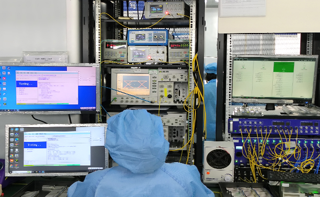
Performance Testing
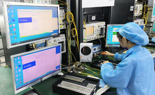
Each module is tested before shipment to help ensure stable optical and electrical performance.
Compatibility Verification
Compatibility validation is available for major switch and router platforms.
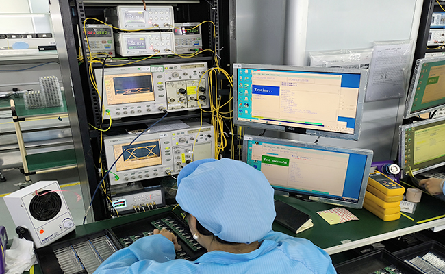
Reliability Screening
Selected products support aging, temperature cycle, and stability testing for demanding applications.
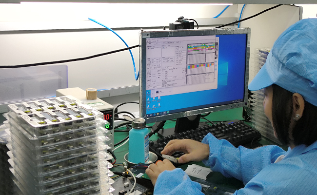
Traceable Quality Control
Inspection and production records support more consistent quality control and batch traceability.
Related products
-
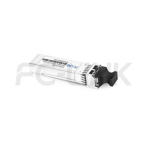
40G QSFP+ SR Transceiver for 150m MMF Links, 850nm MPO8/12
QSFP+40-85-015(SR)-MPO8/12
-
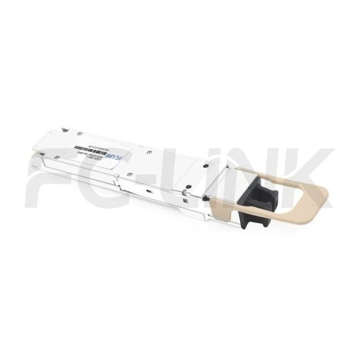
Generic Compatible 400G DR4 QSFP-DD 1310nm 500m DOM MPO8/12 SMF Optical Transceiver Module
QSFPDD-400(4×100)-13-05(DR4)-MPO8/12
-

Generic Compatible 800G DR8 OSFP 500m DOM 2MPO8/12 SMF Optical Transceiver Module
OSFP-800(8x100G)-PAM4-05-(DR8)-MPO16/2MPO8/12
-

16G SFP+ SR Transceiver for 100m MMF Links, 850nm Duplex LC
SFP+16-85-01(SR)-LCD