25G DWDM C-Band SFP28 Transceiver for 10km SMF Links, Duplex LC

SFP28-25-DWC-10-LCD

Category: Tags: , , , , , , Brand:
  • Broad Multi-Brand Compatibility
  • Flexible Customization Support
  • Tested for Reliable Performance
  • Fast Response & Delivery
  • Professional Technical Support

The FC-LINK SFP28 25G DWDM (C Band) 10km LC DX transceiver is a high-performance module designed to deliver 25GBase-DWDM connectivity over single-mode fiber (SMF) for distances up to 10km. Utilizing an LC duplex connector, it provides reliable 25GBASE Ethernet connectivity for 25G Ethernet, telecommunications, and data center applications.This transceiver is fully compliant with SFP28 MSA specifications as well as CPRI and eCPRI standards, ensuring compatibility and seamless integration into modern network infrastructures.

SPECIFICATIONS
Product ModelSFP28-25-DWC-10-LCDManufacturer BrandFC-LINK
Package TypeSFP28Optical ConnectorDuplex LC
Max Data Rate25.78GChannel Data Rate-
Effective Transmission Distance10km
WavelengthC17-C61Operating Voltage3.3V
Fiber TypeSMFCore Size9/125µm
Transmitter TypeEML DWDMReceiver TypePIN
TX Power-2~6dBmReceiver Sensitivity<-12dBm
Digital Optical Monitoring(DOM)YESReceiver Overload-
Power Consumption2WProtocolsMSA, CPRI, eCPRI
Operating Temperature(Commercial)0℃~+70℃Storage Temperature(Commercial)-40℃~+85℃
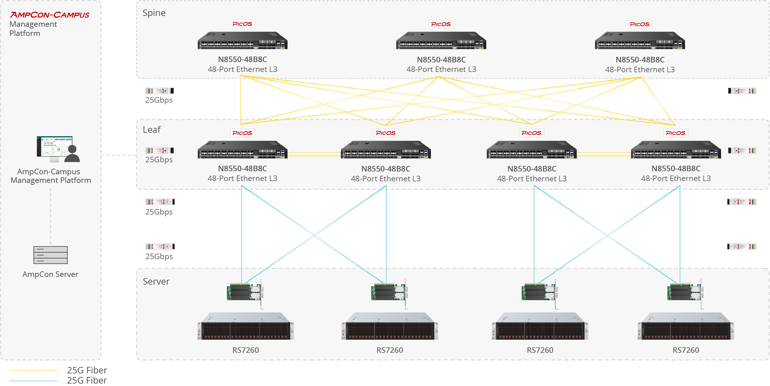
Server-to-Switch Data Center Links

Used for 10G/25G/100G optical uplinks between servers and top-of-rack switches in high-density data center deployments.

Building-to-Building Campus Backbone

Suitable for 1G/10G fiber links between office buildings, campus distribution rooms, and backbone aggregation points.

Access-to-Core Enterprise Uplinks

Designed for switch uplinks from access to aggregation or core layers in enterprise and campus network architectures.

Industrial Switching in Harsh Environments

Applied in industrial Ethernet, automation systems, and outdoor cabinets where wider temperature tolerance and stable fiber communication are required.
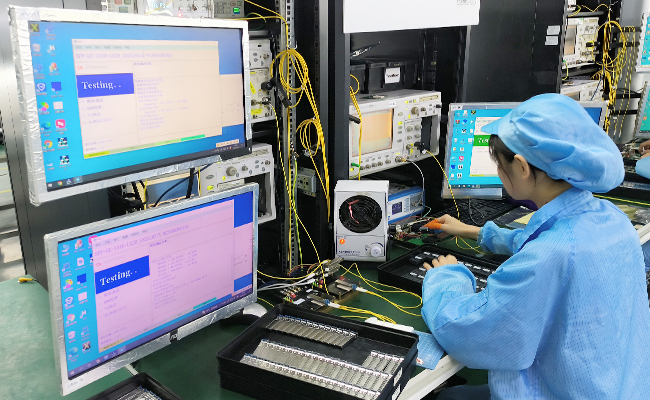

网络拓扑展示模块
1
1
1

Compatible Brands

Customization Options

Vendor Coding
Private Label
Custom Part Number
Packaging Design
Temperature Grade Selection
Absolute Maximum Ratings
Parameter Symbol Min. Max. Unit
Storage temperature  range TS -40  85  °C
Relative humidity RH - 95  %

Recommended Operating Conditions
Parameter Symbol Min. TyP. Max. Unit
Operating case temperature range TC -40  - 85  °C
Power supply voltage VCC 3.14 3.3 3.46 V
Bit rate BR - 25.78125 - Gb/s
Bit error ratio BER - - 5 E-5 -
Max supported link length L - - 10 km

Optical Characteristics
Parameter Symbol Min. Typ. Max. Unit Note
Transmitter
Nominal wavelength λC 1529.55 - 1561.42 nm -
Center wavelength spacing ΔT - 100 - GHz -
Wavelength tolerance ΔCW -80 - 80 pm -
Side mode suppression ratio SMSR 30 - - dB -
Spectral width(-20dB) Δλ - - 0.5 nm -
Average optical power Pavg 0 - 5 dBm -
Extinction ratio ER 6 - - dB -
Mask Margin|5E -5 Margin 10 - - % -
Dispersion Penalty TDP - - 3 dB -
Average optical power of transmitter off Poff - - -30 dBm -
Receiver
Center wavelength λC 1260 - 1620 nm -
Transmitting distance TD   - 10 km -
Average receiver sensitivity Sens - - -18 dBm -
Receiver iverload Rod -5 - - dBm -
Optical return loss ORL 26 - 1561.42 dB -
LOS assert LOSA -35 - - dBm -
LOS de-assert LOSD - - -19 dBm -
LOS hysteresis LOSH 0.5 - 5 dB -

Electrical Characteristics
Parameter Symbol Min. Typ. Max. Unit
Supply voltage VCC 3.14  3.3 3.46 V
Power consumption Por - - 2 W
Transmitter
Input differential impedance Rin 90 100 110 Ω
Differential data input VIN 190 - 700 mVp-p
Transmit disable voltage VDIS 2 - VCCHOST V
Transmit enable voltage VEN VEE - VEE+0.8 V
Transmit fault assert voltage VFA 2 - VCCHOST V
Transmitfault de-assert voltage VFDA VEE - VEE+0.4 V
Receiver
Differential data output VOD 350 - 850 mVp-p
Output rise time@20%~80% tRISE 25 - - PS
Output fall time@20%~80% tFALL 25 - - PS
LOS fault VLOSFT 2 - VCCHOST V
LOS normal VLOSNR VEE - VEE+0.4 V

PIN DEFINITIONS

PIN DEFINITIONS
Pin Symbol Name Description
1,17,20 VeeT Transmitter signal ground These pins should be connected to signal ground on the host board.
TX fault Transmitter fault out(OC) Logic“1 ”output = laser fault (laser off before t_fault)
Logic“0”output = normal operation
This pin is open collector compatible, and should be pulled up to Host Vcc with a 10k Ω resistor.
TX disable Transmitter disable in(LVTTL) Logic“1 ”input (or no connection) = Laser off
Logic“0”input = laser on
This pin is internally pulled up to Vc cT with a 10 kΩ resistor.
SDA Module definition identifiers Serial ID with S FF 8472 diagnostics module Definition pins should be pulled up to Host Vcc with 10kΩ resistors.
SCL
MOD_ABS
RS0 Receiver rate select (LVTTL)
Transmitter rate select (LVTTL)
These pins have an internal 30k Ω pull-down to ground. A signal on either of these pins will not affect module performance.
RS1
LOS Loss of signal out(OC) Sufficient optical signal for potential
BER < 1 x 1 0- 1 2 = Logic“0”
Insufficient optical signal for potential
BER < 1 x 1 0- 1 2 = Logic“1 ”
This pin is open collector compatible, and should be pulled up to Host Vcc with a 1 0k Ω resistor.
10,11,14 VeeR Receiver signal ground These pins should be connected to signal ground on the host board.
12  RD- Receiver negative DATA out(CML) Light on = logic“0”output receiver DATA out put is internally AC coupled and series termin ated with a 50Ω resistor.
13  RD+ Receiver positive DATA out (CML) Light on = Logic“1 ”Output Receiver DATA output is internally AC coupled and series terminated with a 50Ω resistor.
15  VccR Receiver power supply This pin should be connected to a filtered +3.3V power supply on the host board.See Figure 3.recommended power supply filter
16  VccT Transmitter power supply This pin should be connected to a filtered +3.3V power supply on the host board.See Figure 3.Recommended power supply filter
18  TD+ Transmitter positive DATA in (CML) Logic“1 ”Input = Light on Transmitter DATA inputs are
internally AC coupled and terminated with a differential
100 Ω resistor.
19  TD- Transmitter negative DATA in (CML) Logic“0”Input = Light on Transmitter DATA inputs are
internally AC coupled and terminated with a differential
100 Ω resistor.

DDM ACCURACY
Parameter Symbol Min . Max. Unit
Temperature Tc -3 3
Voltage Vc -3 3 %
Ibias Icc -10 10 %
Tx power TXPWR -3 3 dB
Rx power RXPWR -3 3 dB

Performance Testing

Each module is tested before shipment to help ensure stable optical and electrical performance.

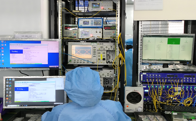
Compatibility Verification

Compatibility validation is available for major switch and router platforms.

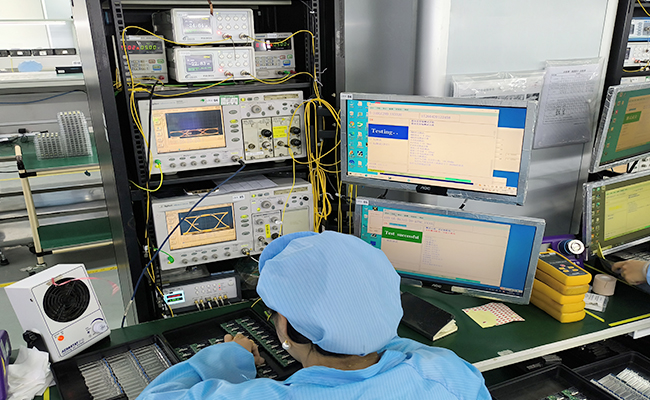
Reliability Screening

Selected products support aging, temperature cycle, and stability testing for demanding applications.

Traceable Quality Control

Inspection and production records support more consistent quality control and batch traceability.

光模块产品详情订购信息---SFP28(CWDM/DWDM/LWDM)