


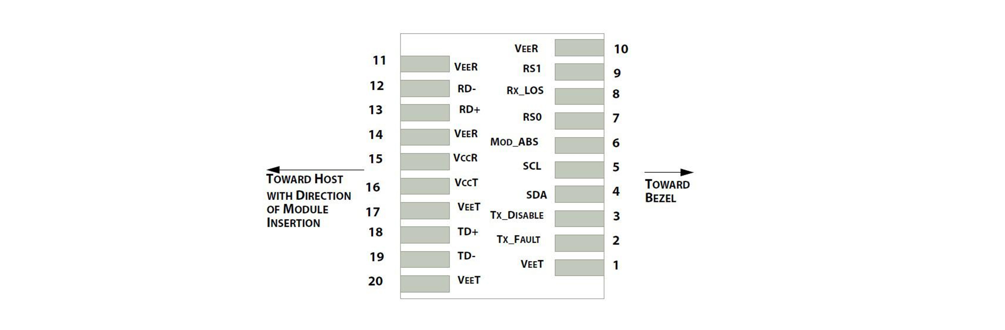
25G SFP28 ER Transceiver for 30km SMF Links, 1310nm Duplex LC
SFP28-25-13-30(ER)-LCD
- Broad Multi-Brand Compatibility
- Flexible Customization Support
- Tested for Reliable Performance
- Fast Response & Delivery
- Professional Technical Support
The FC-LINK SFP28 25G 1310nm 30km ER LC DX transceiver is specifically designed for Ethernet links, supporting data rates of up to 25.78 Gb/s and a transmission distance of up to 30km without FEC. It adheres to SFF-8472 standards and is compatible with SFF-8432 and relevant sections of SFF-8431. Additionally, the product is RoHS-compliant and lead-free in accordance with Directive 2011/96/EU.
| SPECIFICATIONS | |||
|---|---|---|---|
| Product Model | SFP28-25-13-30(ER)-LCD | Manufacturer Brand | FC-LINK |
| Package Type | SFP28 | Optical Connector | Duplex LC |
| Max Data Rate | 25.78G | Channel Data Rate | 10.31Gbps |
| Effective Transmission Distance | 30km | ||
| Wavelength | 1310nm | Operating Voltage | 3.3V |
| Fiber Type | SMF | Core Size | 9/125µm |
| Transmitter Type | EML | Receiver Type | APD |
| TX Power | 0~6dBm | Receiver Sensitivity | <-19dBm |
| Digital Optical Monitoring(DOM) | YES | Receiver Overload | -5dBm |
| Power Consumption | ≤1.5W | Protocols | MSA, CPRI, eCPRI1 |
| Operating Temperature(Commercial) | 0℃~+70℃ | Storage Temperature(Commercial) | -40℃~+85℃ |

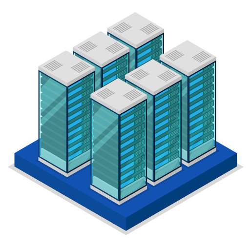
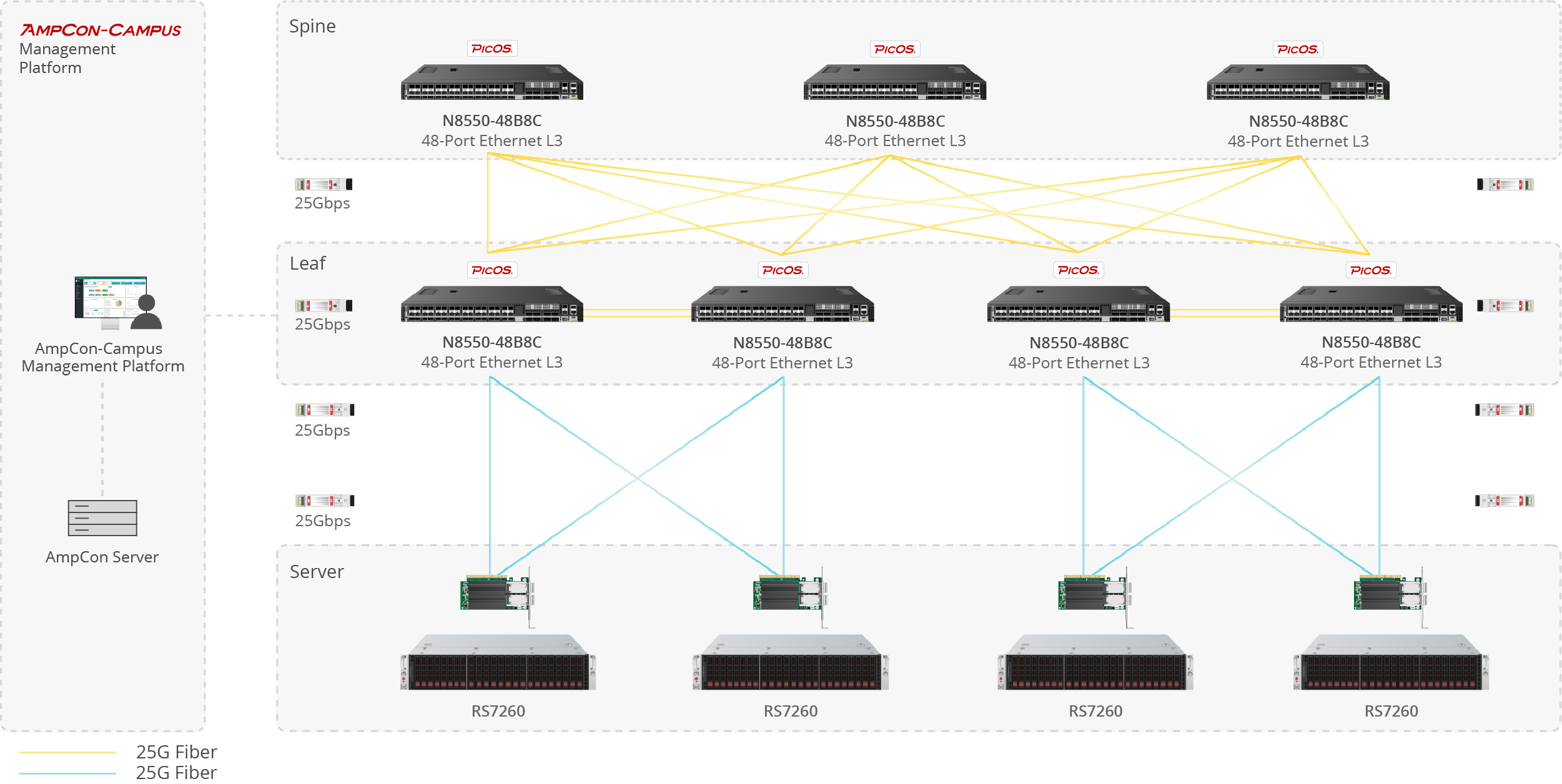
Server-to-Switch Data Center Links
Used for 10G/25G/100G optical uplinks between servers and top-of-rack switches in high-density data center deployments.

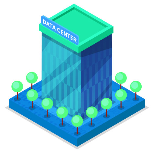
Building-to-Building Campus Backbone
Suitable for 1G/10G fiber links between office buildings, campus distribution rooms, and backbone aggregation points.

Access-to-Core Enterprise Uplinks
Designed for switch uplinks from access to aggregation or core layers in enterprise and campus network architectures.

Industrial Switching in Harsh Environments
Applied in industrial Ethernet, automation systems, and outdoor cabinets where wider temperature tolerance and stable fiber communication are required.
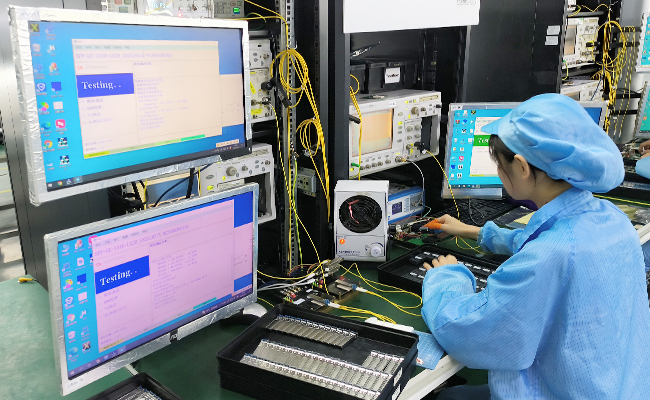
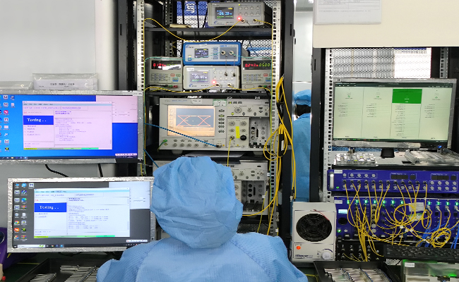
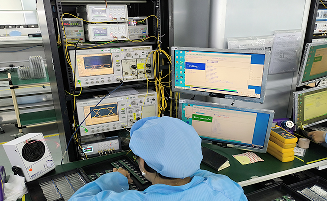
| Absolute Maximum Ratings | |||||||||
| Parameter | Symbol | Min. | Typ. | Max. | Unit | ||||
| Storage temperature | TS | -40 | - | 85 | °C | ||||
| Case operating temperature | TA | 0 | - | 70 | °C | ||||
| Maximum supply voltage | Vcc | 0 | - | 3.6 | V | ||||
| Relative humidity | RH | 0 | - | 85 | % | ||||
| Electrical Characteristics | |||||||||
| Parameter | Symbol | Min. | Typ. | Max. | Unit | Note | |||
| Supply voltage | VCC | 3.15 | - | 3.46 | V | - | |||
| Supply current | Icc | - | - | 450 | mA | - | |||
| Power consumption | P | - | - | 1.5 | W | - | |||
| Data rate | R | - | 25.8 | - | Gb/s | - | |||
| Transmitter | |||||||||
| Input differential impedance | Rin | - | 100 | - | Ω | 1 | |||
| Differential input voltage swing | Vin,pp | 180 | - | 700 | mV | 2 | |||
| Transmit disable voltage | VD | 2 | - | Vcc | V | 3 | |||
| Transmit enable voltage | VEN | Vee | - | Vee+0.8 | V | - | |||
| Receiver | |||||||||
| Single ended output voltage tolerance |
V | -0.3 | - | 4 | V | - | |||
| Rx output diff voltage | Vo | 185 | - | 800 | mV | - | |||
| LOS fault | VLOS fault | 2 | - | VccHOST | V | 4 | |||
| LOS normal | VLOS norm | Vee | - | Vee+0.8 | V | 4 | |||
| Notes: 1.Connected directly to TX data input pins. AC coupling from pins into laser driver IC. 2.Per SFF-8431 Rev 3.0 3.Into 100 ohms differential termination. 4.LOS is an open collector output. Should be pulled up with 4.7k – 10kΩ on the host board. Normal operation is logic 0; loss of signal is logic 1. Maximum pull-up voltage is 5.5V. |
|||||||||
| Optical Characteristics | |||||||||
| Parameter | Symbol | Min. | Typ. | Max | Unit | Notes | |||
| Transmitter | |||||||||
| Center wavelength | λt | 1295 | - | 1325 | nm | - | |||
| Spectral width | △λ | - | - | 1 | nm | - | |||
| Average optical power | Pavg | 0 | - | +6 | dBm | 1 | |||
| Laser off power | Poff | - | - | -30 | dBm | - | |||
| Side mode suppression ratio | - | 30 | - | - | - | - | |||
| Extinction ratio | ER | 4 | - | - | dB | - | |||
| Optical return loss tolerance | - | - | - | -12 | dB | - | |||
| Receiver | |||||||||
| Center wavelength | λr | 1260 | - | 1370 | nm | - | |||
| Receiver sensitivity | Sen | - | - | -19 | dBm | 2 | |||
| Los assert | LOSA | -30 | - | - | dBm | - | |||
| Los dessert | LOSD | - | - | -19 | dBm | - | |||
| Los hysteresis | LOSH | 0.5 | - | - | dB | - | |||
| Overload | - | -6 | - | - | dBm | - | |||
| Notes: 1.Average power figures are informative only, per IEEE802.3CC. 2.Receiver sensitivity is informative. Shall be measured with conformance test signal for . BER =5x 10⁻⁵. |
|||||||||
| Timing Characteristics | |||||||||
| Parameter | Symbol | Min. | Typ. | Max. | Unit | ||||
| TX_disable assert time | t_off | - | - | 100 | us | ||||
| TX_disable negate time | t_on | - | - | 2 | ms | ||||
| Time to initialize 2-wire interface | t_2w_start_up | - | - | 300 | ms | ||||
| Time to initialize | t_start_up | - | - | 300 | ms | ||||
| Time to initialize cooled module and time to power up a cooled module to power level II | t_start_up_cooled | - | - | 90 | s | ||||
| Time to power up to level II | t_power_level2 | - | - | 300 | ms | ||||
| Time to power down from level II | t_power_down | - | - | 300 | ms | ||||
| Tx_fault assert | Tx_Fault_on | - | - | 1 | ms | ||||
| Tx_fault assert for cooled module | Tx_Fault_on_cooled | - | - | 50 | ms | ||||
| TX_FAULT reset | t_reset | 10 | - | - | us | ||||
| Rx_LOS assert delay | t_los_on | - | - | 100 | us | ||||
| Rx_LOS negate delay | t_los_off | - | - | 100 | us | ||||
| Digital Diagnostic Specifications | |||||||||
| Parameter | Symbol | Min. | Max. | Accuracy | Unit | ||||
| Transceiver temperature | T | 0 | +70 | ±3.0°C | °C | ||||
| Transceiver supply voltage | DDVoltage | 3.15 | 3.45 | ±3% | V | ||||
| Transmitter bias current | DDBias | 0 | 35 | ±10% | mA | ||||
| Transmitter output power | DDTx-Power | -5 | +5 | ±2dB | dBm | ||||
| Receiver average optical input power | DDRx-Power | -16 | -3 | ±2dB | dBm | ||||
| Pin Description |
| Pin | Symbol | Name/Description | Plug Seq. | ||||||
| 1 | VeeT | Module transmitter ground | 1 | ||||||
| 2 | TX fault | Module transmitter fault | 2 | ||||||
| 3 | TX disable | Transmitter disable; turns off transmitter laser output | 3 | ||||||
| 4 | SDL | 2 wire serial interface data input/output (SDA) | 4 | ||||||
| 5 | SCL | 2 wire serial interface clock input (SCL) | 4 | ||||||
| 6 | MOD_ABS | Module absent, connect to VeeR or VeeT in the module | 2 | ||||||
| 7 | RS0 | Rate select0: module inputs and are pulled low to VeeT with >30kΩ resistorsin the module. | - | ||||||
| 8 | LOS | Receiver Loss of signal indication | - | ||||||
| 9 | RS1 | Rate select1: module inputs and are pulled low to VeeT with >30kΩ resistorsin the module. | - | ||||||
| 10 | VeeR | Module receiver ground | 1 | ||||||
| 11 | VeeR | Module receiver ground | 1 | ||||||
| 12 | RD- | Receiver inverted data out put | - | ||||||
| 13 | RD+ | Receiver non-inverted data out put | - | ||||||
| 14 | VeeR | Module receiver ground | 1 | ||||||
| 15 | VccR | Module receiver 3.3V supply | - | ||||||
| 16 | VccT | Module transmitter 3.3V supply | - | ||||||
| 17 | VeeT | Module transmitter ground | 1 | ||||||
| 18 | TD+ | Transmitter non-inverted data out put | - | ||||||
| 19 | TD- | Transmitter inverted data out put | - | ||||||
| 20 | VeeT | Module transmitter ground | 1 | ||||||
| Notes: 1.The module ground pins shall be isolated from the module case. 2.This pin is an open collector/drain output pin and shall be pulled up with 4.7K-10Kohms to Host_Vcc on the host board. 3.This pin shall be pulled up with 4.7K-10Kohms to VccT in the module. 4.This pin is an open collector/drain output pin and shall be pulled up with 4.7K-10Kohms to Host_Vcc on the host board. |
|||||||||
Diagram of Host Board Connector Block Pin Numbers and Names

Performance Testing
Each module is tested before shipment to help ensure stable optical and electrical performance.

Compatibility Verification
Compatibility validation is available for major switch and router platforms.

Reliability Screening
Selected products support aging, temperature cycle, and stability testing for demanding applications.

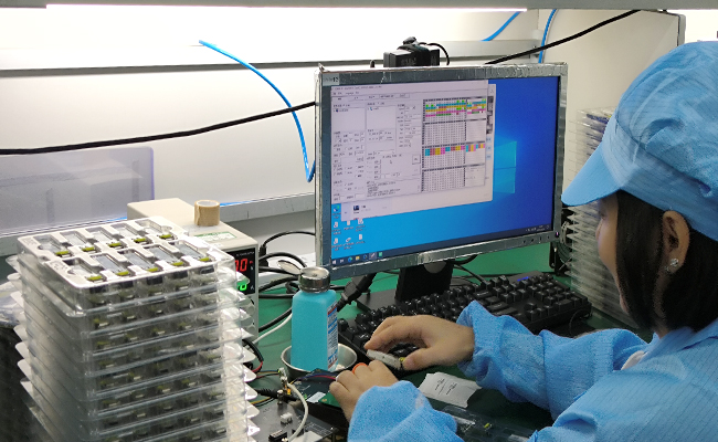
Traceable Quality Control
Inspection and production records support more consistent quality control and batch traceability.


