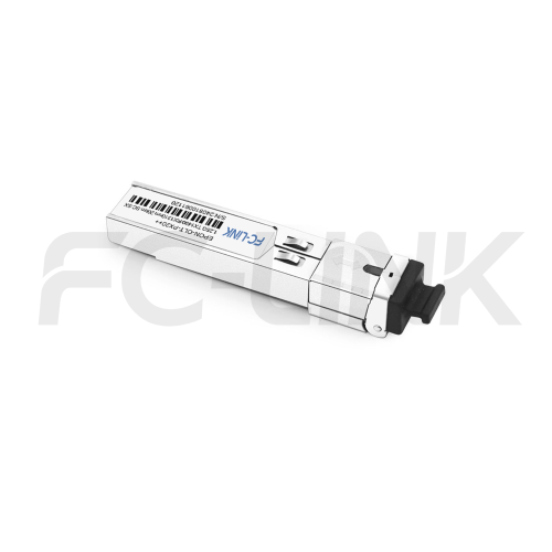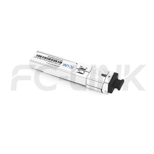
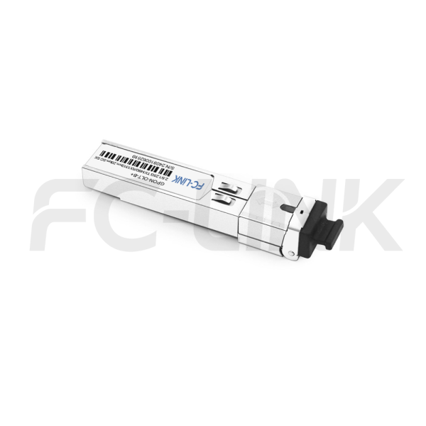
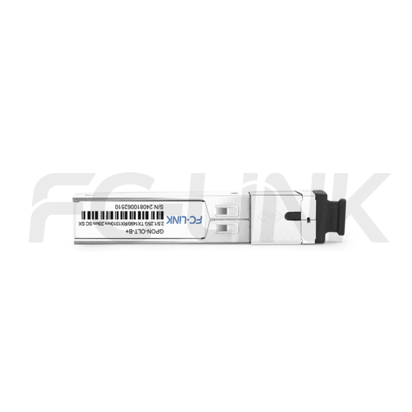
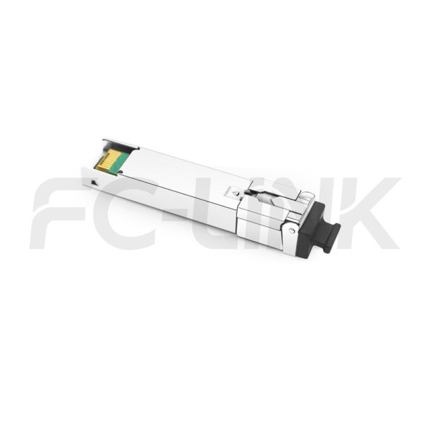
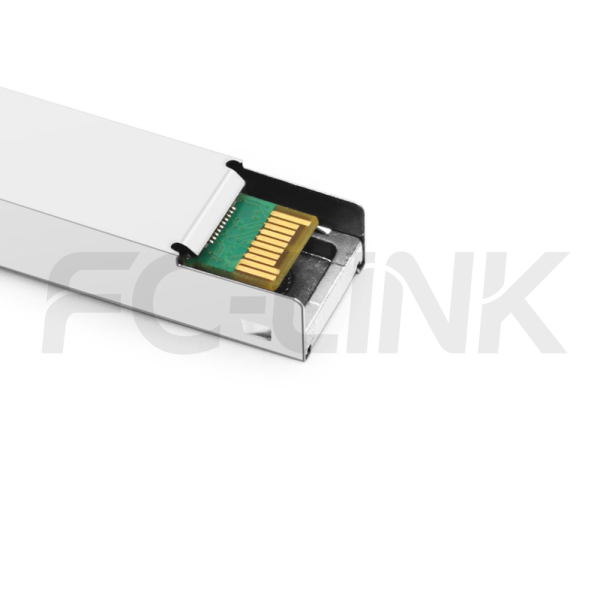
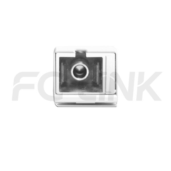
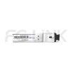
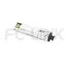
2.5/1.25G SFP B+ GPON OLT Transceiver for 20km SMF Links, 1490/1310nm Simplex SC

SFP-GPON-B+2.5/1.25-1413-20-SCS

  • Broad Multi-Brand Compatibility
  • Flexible Customization Support
  • Tested for Reliable Performance
  • Fast Response & Delivery
  • Professional Technical Support

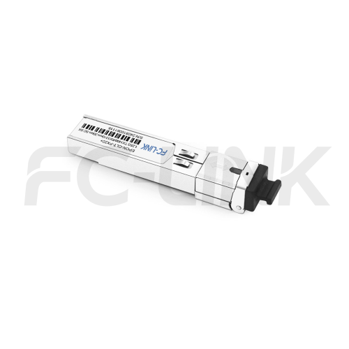
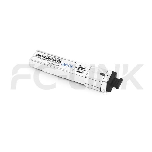
The FC-LINK GPON OLT B+ 3dBm Transceiver is a SFP module engineered for Optical Line Terminal applications, delivering asymmetric transmission at 2.488Gbps downstream (1490nm) and 1.244Gbps upstream (1310nm) over single-mode fiber with 20km reach. Featuring an SC/UPC connector and compliant with the GPON B+ class (3dBm optical budget), this transceiver integrates bidirectional communication on a single fiber while supporting Digital Diagnostic Monitoring (DDM) per SFF-8472 for real-time performance tracking. It fully meets ITU-T G.984.2 standards and RoHS compliance requirements.

SPECIFICATIONS
Product ModelSFP-GPON-B+2.5/1.25-1413-20-SCSManufacturer brandFC-LINK
Package TypeSFPOptical connectorSC
Max Data Rate2.5/1.25GbpsClassB+
Effective transmission distance20KM
Wavelength1310nm/1490nm
1490nm/1310nm
Operating voltage3.3V
Fiber TypeSMFCore Size9/125µm
Transmitter TypeDFBReceiver TypeAPD
TX Power2.5~3dBmReceiver Sensitivity-30dBm
Digital Diagnostic Monitoring(DDM)YESReceiver Overload-8dBm
Power Consumption<1WProtocolsSFP MSA SFF-8472
Operating temperature(Commercial)0℃~+70℃Storage Temperature(Commercial)-40℃~+85℃
Operating temperature(Industrial)-40℃~+85℃Storage Temperature(Industrial)-40℃~+85℃
Data center optical transceiver application scenario
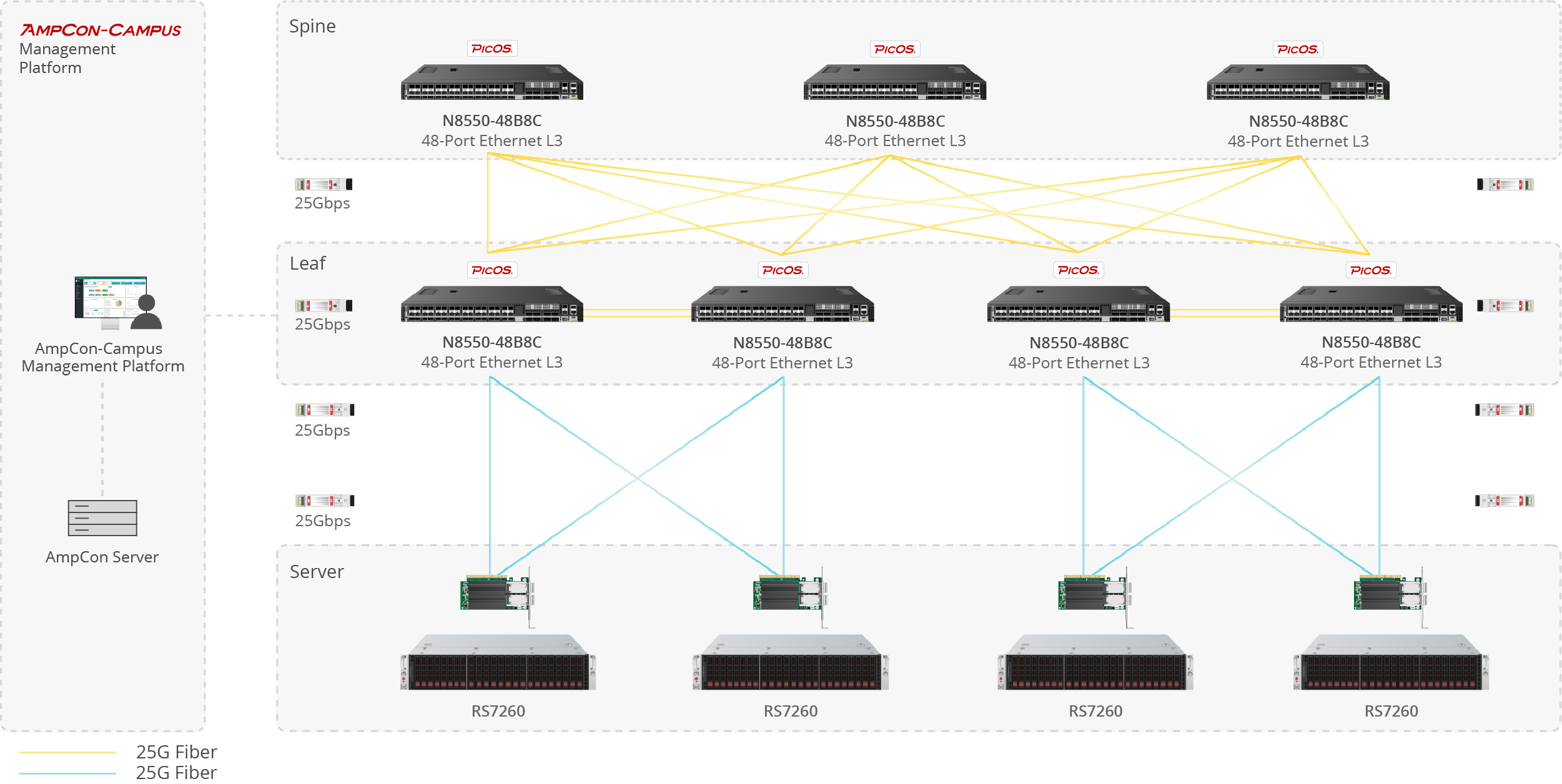
Server-to-Switch Data Center Links

Used for 10G/25G/100G optical uplinks between servers and top-of-rack switches in high-density data center deployments.

Enterprise network fiber optic application scenario
Building-to-Building Campus Backbone

Suitable for 1G/10G fiber links between office buildings, campus distribution rooms, and backbone aggregation points.

Telecom fiber optic link application scenario
Access-to-Core Enterprise Uplinks

Designed for switch uplinks from access to aggregation or core layers in enterprise and campus network architectures.

Industrial fiber optic network application scenario
Industrial Switching in Harsh Environments

Applied in industrial Ethernet, automation systems, and outdoor cabinets where wider temperature tolerance and stable fiber communication are required.


1
1
1

Compatible Brands

Customization Options

Vendor Coding
Private Label
Custom Part Number
Packaging Design
Temperature Grade Selection
ParameterSymbolMin.Max.Unit
Storage TemperatureTS-4085
Operating TemperatureTop070
Supply VoltageVCC-0.53.6V
Power Supply CurrentICC-400mA
Voltage at Any Input PinVIN0VccV
Recommended Operating Environment
ParameterSymbolMin.TypicalMax.Unit
Operating TemperatureTop0-70
Supply VoltageVCC3.13.33.5V
Tx Data Rate--2488-Mb/s
Rx Data Rate--1244-Mb/s
Electrical
ParameterSymbolMin.Typ.Max.Unit
Transmitter(T=0 to +70℃, VCC =3.1~3.5V)
Central WavelengthλC148014901500nm
Spectral WidthΔλ--1nm
Side Mode Suppression RatioSMSR30--dB
Output PowerPo2.5-3dBm
Extinction RatioER8.2--dB
Output Power at Transmit Off----40dBm
Differential Input VoltageVIH- VIL200-1600mV
TX Disable Input Voltage LowTX_DISABLEL0-0.8V
TX Disable Input Voltage HighTX_DISABLEH2-VccV
TX Fault Output Voltage LowTX_FAULTL0-0.8V
TX Fault Output Voltage HighTX_FAULTH2-VCC+0.3V
Eye DiagramCompliance with ITU-T G.984.2
Receiver(T=0 to +70℃, VCC =3.1~3.5V)
Wavelength Rangeλ1260-1360nm
MIN. Input Power (Sensitivity)PMIN---30dBm
MAX. Input Power (Saturation)PMAX-12--dBm
Signal Detect-AssertedPA---30dBm
Signal Detect-DeassertedPD-45--dBm
Signal Detect HysteresisPHYS0.5-6dB
Return LossORL12--dB
RX Loss of Signal Output Voltage LowRX_LOSL0-0.8V
RX Loss of Signal Output Voltage HighRX_LOSH2-VCC+0.3V
LOS Assert TimeTAssert--100ns
LOS De-assert TimeTDeassert--12.8ns
Digital RSSI Timing Specification
ParameterMinimumTypicalMaximumUnitNotes
RSSI Trigger Delay25--ns-
RSSI Sampling Time300--ns-
Internal I2C Delay--500us-
Receiver Power DDM(RSSI) Error--+/-3dB-
a) RSSI_ACQ input signal rising edge will trigger RSSI sampling, and falling edge will trigger internal digital RSSI information written to I2C. It is recommended that host shall not trigger RSSI_ACQ input again until RSSI data is valid inI2C from previous RSSI trigger.

b) RSSI DDM working range is between -8 to -28dBm. RSSI DDM accuracy is better than +/-3dB for input power level between -10 to -28dBm, the accuracy reduces to +/-5dBm to -10 dBm. If the data pattern is at least 2^7-1 or longer, a minimum average of 8 times is strongly recommended to maintain the RSSI reading accuracy.
EEPROM Serial ID Memory Contents (A0h)
AddressSize(Bytes)Name of FieldHexDescription of Field
01Identifier3SFP
11Ext. Identifier4MOD4
21Connector1SC
3—108Transceiver00 00 00 00 00 00 00 00Transceiver Code Field,not applicable
111Encoding3NRZ encoding
121BR, nominal192488.32Mbps
131Reserved0Reserved
141Length(9um)-km1420(Units of km)
151Length (9um)C8200(Units of 100 m)
161Length (50um)0Not Support MMF
171Length (62.5um)0Not Support MMF
181Length (copper)0Not Support Copper
191Reserved0-
20—3516Vendor nameXXXXX“ODI”
361Reserved0-
37—393Vendor OUI0-
40—5516Vendor PNXXXXX“PART NUMBER ” (ASCⅡ)
56—594Vendor revxxxx xxxxASCⅡ (“31 2E 31 20” means 1. 1 revision)
60-612Wavelength05 D21490nm Laser wavelength
621Reserved0-
631CC BASExxChecksum of bytes 0 - 62
64—652Options00 1ALOS, TX_FAULT and TX_DISABLE
661BR, max0-
671BR, min0-
68—8316Vendor SNxxxx xxxx xxxx xxxx
xxxx xxxx xxxx xxxx
SN :xxxxxxxxx (ASCⅡ)
84—918Vendor date codexxxx xxxx xxxx 20 20Year (2 bytes), Month (2 bytes), Day (2 bytes) (ASCⅡ)
921Diagnostic type58Externally Calibrated
931Enhanced optionB0Diagnostic(Optional Alarm/warning flags)
Soft TX_FAULT monitoring implemented
Soft RX_LOS monitoring implemented
941SFF-84721Includes functionality described in Rev 9. 4
SFF-8472
951CC_EXTxxChecksum of bytes 64 - 94
96—12732Vendor specific-Vendor Specific EEPROM
128-255128Reserved-Reserved for future use.
Note:
1.The“ xx” byte should be filled in according to practical case.
2. Note that, A0H is readable and writeable , A2H is readable and write-protected.
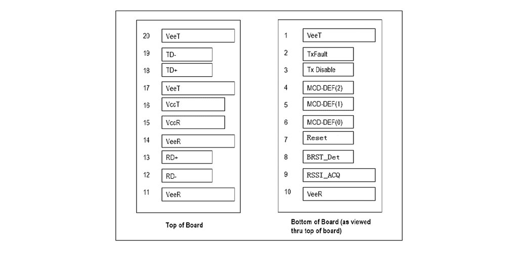
Function Definition

Function Definition
Pin No.NameFunctionPlug Seq.Notes
1VeeTTx Ground1-
2TX FaultTransmitter Fault Indication,LVTTL Output Active High3Note 1
3TX DisableTransmitter Disable,LVTTL input.3Note 2
4MOD-DEF22-Write Serial Data I/O Pin.3Note 3
5MOD-DEF12-Write Serial Data I/O Pin.3Note 3
6MOD-DEF0Internally Grounded3Note 3
7ResetCMOS input.Assert “Reset”high at the end of previous burst,2 byte in duration3-
8BRST_DetLVTTL output.BRST_Det assert low when module receives“reset”signal, assert high when incoming burst is present.3Note 4
9RSSI_ACQRSSI acquire/hold LVTTL input. Digital RSSI output through I2C1-
10VeeRReceiver Ground1-
11VeeRReceiver Ground1-
12RD-Inv. Received Data Out3Note 5
13RD+Received Data Out3Note 5
14VeeRReceiver Ground1-
15VccRReceiver Power2-
16VccTTransmitter Power2-
17VeeTTransmitter Ground1-
18TD+Transmit Data In3Note 6
19TD-Inv Transmit Data In3Note 6
20VeeTTransmitter Ground1-
Notes:
1. TX Fault is an open collector output, which should be pulled up with a 4.7K~10KΩ resistor on the host board to a voltage between 2.0V and Vcc+0.3V. Logic 0 indicates normal operation; logic 1 indicates a laser fault of some kind. In the low state, the output will be pulled to less than 0.8V.

2. TX Disable is an input that is used to shut down the transmitter optical output. It is pulled up within the module with a 4.7K~10KΩ resistor. Its states are:
Low (0~0.8V): Transmitter on
(>0.8V, <2.0V): Undefined
High (2.0~3.465V): Transmitter Disabled
Open:Transmitter Disabled.

3. MOD-DEF 0,1,2 are the module definition pins. They should be pulled up with a 4.7K~10KΩ resistor on the host board. The pull-up voltage shall be VccT or VccR.
MOD-DEF 0 is grounded by the module to indicate that the module is present.
MOD-DEF 1 isthe clock line of two wire serial interface for serial ID.
MOD-DEF 2 isthe data line of two wire serial interface for serial ID.

4. LOS is an open collector output, which should be pulled up with a 4.7K~10KΩ resistor on the host board to a voltage between 2.0V and Vcc+0.3V. Logic 0 indicates normal operation; logic 1 indicates loss of signal. In the low state, the output will be pulled to less than 0.8V.

5. These are the differential receiver outputs. They are AC coupled 100Ω differential lines which should be terminated with 100Ω (differential) atthe user SERDES.

6. These are the differential transmitter inputs. They are AC-coupled, differential lines with 100Ω differential termination inside the module.
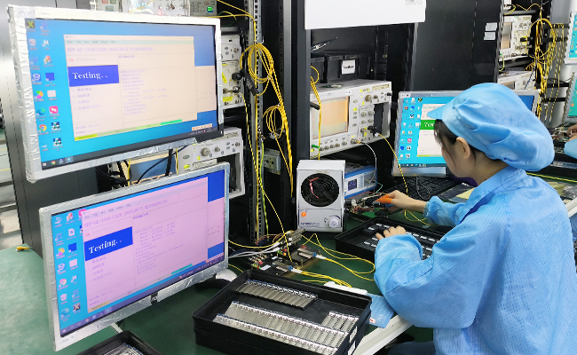
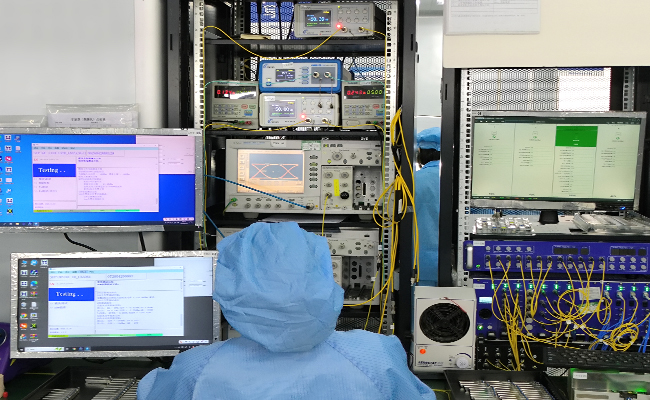
Optical transceiver TX RX performance test
Performance Testing

Each module is tested before shipment to help ensure stable optical and electrical performance.
Optical transceiver compatibility test
Compatibility Verification

Compatibility validation is available for major switch and router platforms.
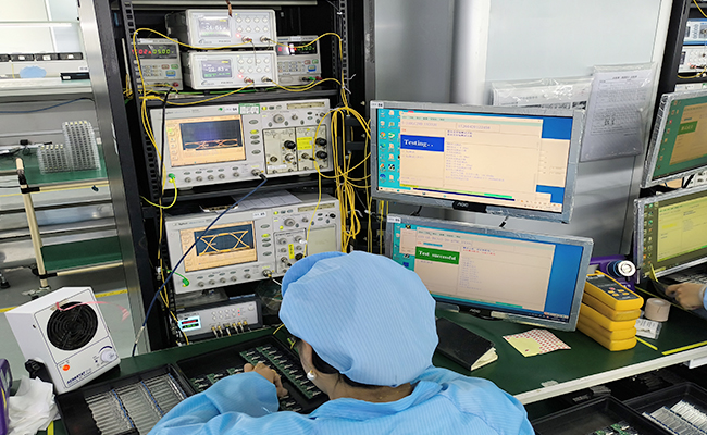
Optical transceiver aging and reliability test
Reliability Screening

Selected products support aging, temperature cycle, and stability testing for demanding applications.
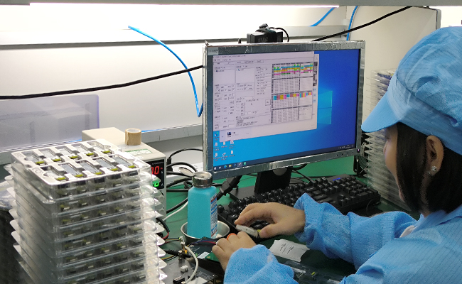
Automatic labeling and traceability for optical transceivers
Traceable Quality Control

Inspection and production records support more consistent quality control and batch traceability.

光模块产品详情订购信息---QSFP+