40G CWDM4 QSFP+ LR4 Transceiver for 10km SMF Links, Duplex LC

QSFP+40-CW4-10(LR4)-LCD

Category: Tags: , , , , , Brand:
  • Broad Multi-Brand Compatibility
  • Flexible Customization Support
  • Tested for Reliable Performance
  • Fast Response & Delivery
  • Professional Technical Support

The FC-LINK QSFP+ 40G CWDM4 10km LR4 LC DX transceiver is engineered for 40GBASE Ethernet connections, supporting up to 10 kilometers over single-mode fiber (SMF) at a 1310nm wavelength, using duplex LC connectors. It complies with QSFP+ MSA, IEEE 802.3ba 40GBASE-LR4, and OTU3 C4S1-2D1 standards. Additionally, it offers digital diagnostics through the I2C interface as outlined by the QSFP+ MSA, enabling real-time monitoring of operating parameters. This hot-swappable, easy-to-install transceiver is ideal for use in data centers, high-performance computing, and enterprise core and distribution networks.

SPECIFICATIONS
Product ModelQSFP+40-CW4-10(LR4)-LCDManufacturer BrandFC-LINK
Package TypeQSFP+Optical ConnectorLC Duplex
Max Data Rate40GbpsChannel Data Rate10Gbps
Effective Transmission Distance10km
Wavelength1271nm
1291nm
1311nm
1331nm
Operating Voltage3.3V
Fiber TypeSMFCore Size9/125µm
Transmitter TypeDFBsReceiver TypePIN
TX Power-7~+2.3dBmReceiver Sensitivity< -11.5dBm
Digital Diagnostic Monitoring(DDM)YESReceiver Overload2.3dBm
Power Consumption≤3.5WProtocolsIEEE 802.3ba(40GBASE-LR4)
Operating Temperature(Commercial)0℃~+70℃Storage Temperature(Commercial)-40℃~+85℃
Operating Temperature(Industrial)-40℃~+85℃Storage Temperature(Industrial)-40℃~+85℃
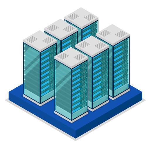
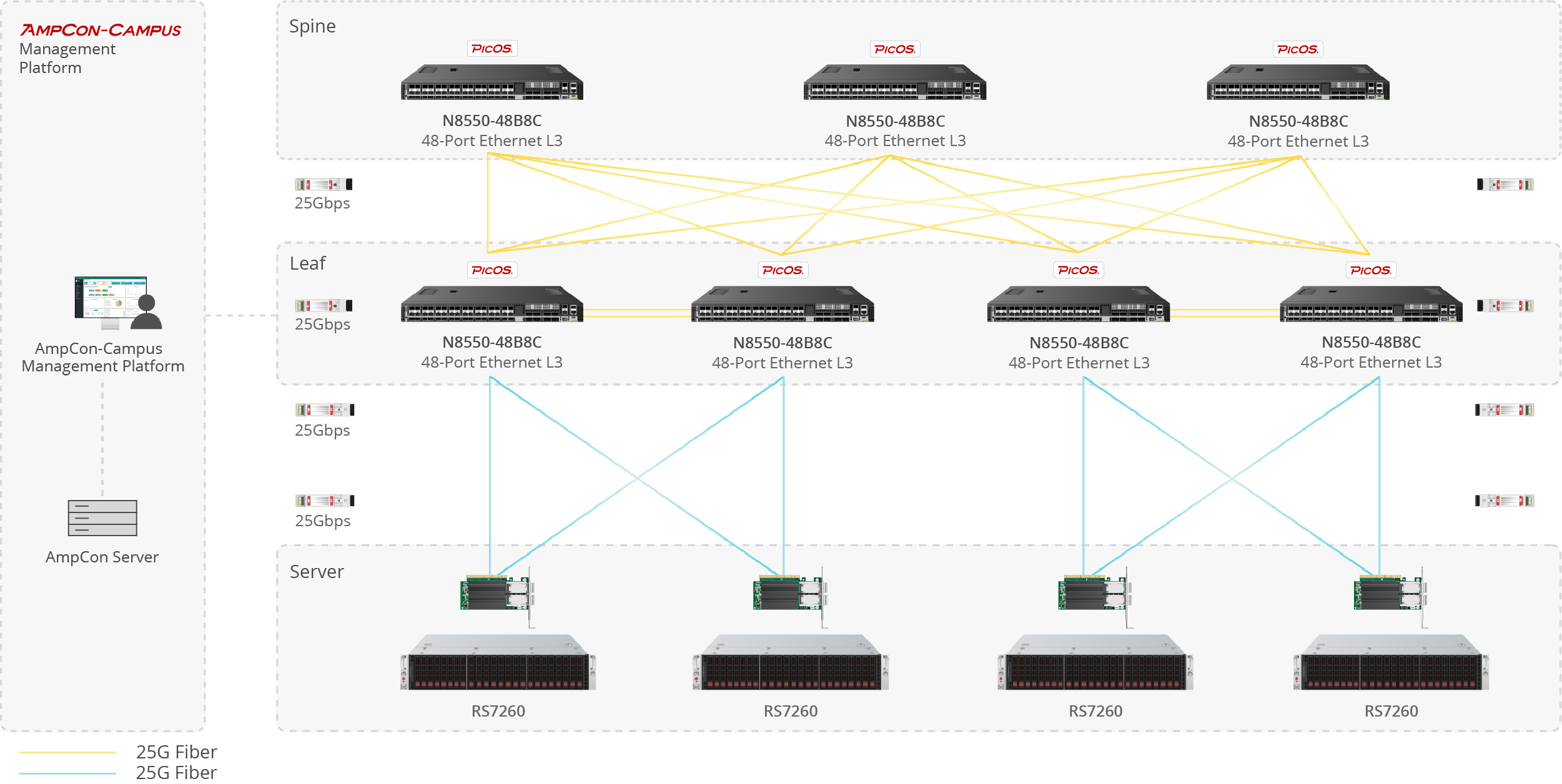
Server-to-Switch Data Center Links

Used for 10G/25G/100G optical uplinks between servers and top-of-rack switches in high-density data center deployments.

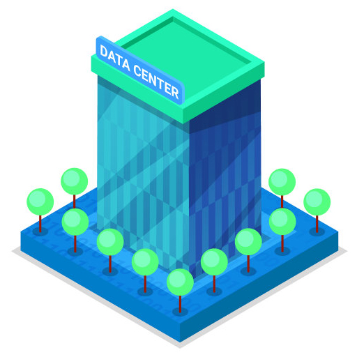
Building-to-Building Campus Backbone

Suitable for 1G/10G fiber links between office buildings, campus distribution rooms, and backbone aggregation points.

Access-to-Core Enterprise Uplinks

Designed for switch uplinks from access to aggregation or core layers in enterprise and campus network architectures.

Industrial Switching in Harsh Environments

Applied in industrial Ethernet, automation systems, and outdoor cabinets where wider temperature tolerance and stable fiber communication are required.
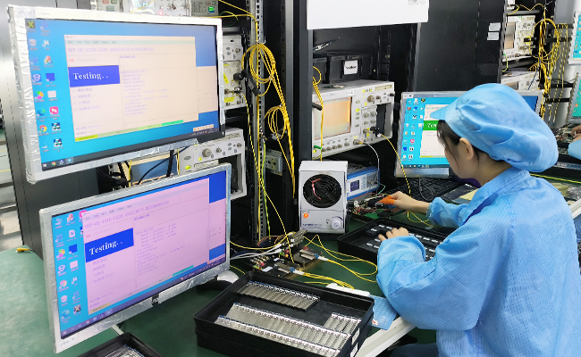

网络拓扑展示模块
1
1
1

Compatible Brands

Customization Options

Vendor Coding
Private Label
Custom Part Number
Packaging Design
Temperature Grade Selection
Absolute Maximum Ratings
Parameter Symbol Min. Max. Unit
Storage temperature TS -40 +85 °C
Supply voltage VCC -0.5 3.6 V
Operating relative humidity RH 0 85 %
  *Exceeding any one of these values may destroy the device immediately.

Recommended Operating Conditions
Parameter Symbol Min. Typical Max. Unit
Operating case temperature Tc 0 - +70 °C
Power supply voltage Vcc 3.15 3.3 3.45 V
Power supply current Icc - - 1100 mA
Power dissipation PD - - 3.5 W
Aggregate bit rate BRAVE - 41.25(40GE)
43.018(OTU3)
- Gbps
Lane bit rate BRLANE - 10.3125(40GE)
10.7546(OTU3)
- Gbps

Performance Specifications-Electrical
Parameter    Symbol Min. Typ. Max Unit Notes
Transmitter
Single ended input voltage tolerance - -0.3 -    4 V Referred to TP1 signal common
Differential input amplitude - 150 - 1000 mvp-p  
AC common mode input voltage tolerance - 15 - - mV RMS
Input impedance(differential) Zin 85   100 115 ohms Rin > 100 kohms @ DC
TX Disable Disable VIH 2 - Vcc+0.3 V -
Enable VIL 0 - 0.8 -
TX FAULT Fault VOH 2.4 - Vcc+0.3 V -
Normal VOL 0 - 0.8 -
Receiver
Single ended output voltage - -0.3 - 4 s Referred to ignal common
Differential output amplitude - 290 - 1000 mvp-p -
AC common mode voltage - - - 7.5 mV RMS
Termination mismatch at 1MHz - - - 5 % -
Output impedance(differential) Zout 85   100 115 ohms -
Output rise/fall time tr/tf 30 - - ps 10%~90%
  RX_LOS LOS VOH 2.4 - Vcc+0.3 V -
Normal VOL 0 - 0.8 V -

Optical and Electrical Characteristics
Parameter Symbol Min. Typical Max. Unit
SMF L - 10 - km
Aggregate bit rate BRAVE - 41.25 - Gbps
Per lane bit rate BRLANE - 10.3125 - Gbps
Transmitter
Channels wavelength λC 1264.5 1271 1277.5 nm
1284.5 1291 1297.5
1304.5 1311 1317.5
1324.5 1331 1337.5
-20dB spectral width ∆λ - - 1 nm
Average launch power, each lane Pout/lane -7 - 2.3 dBm
Transmit OMA, per lane TX_OMA/lane -4 - 3.5 dBm
Extinction ratio Er 3.5 - - dB
Output optical eye IEEE 802.3ba-2010 Compliant
Receiver
Channels wavelength λC 1264.5 1271 1277.5 nm
1284.5 1291 1297.5
1304.5 1311 1317.5
1324.5 1331 1337.5
Damage threshold - 5.5 - - dBm
Receiver sensitivity in OMA, each lane Pmins - - - 11.5 dBm
Maximum receive power, each lane Pmax 2.3 - - dBm
Receiver reflectance Rr - - -26 dB
Los de-assert LOSD - - - 11.5 dBm
Los assert LOSA -24 - - dBm
Los hysteresis - 0.5 - - dB

Functional Description of Transceiver

QSFP+ Transceiver Electrical Pad Layout

Pin Arrangement And Definition
Pin Logic Symbol Description Plug Sequence Notes
1 - GND Ground 1 1
2 CML-I Tx2n Transmitter Inverted Data Input 3 -
3 CML-I Tx2p Transmitter Non-Inverted Data Input 3 -
4 - GND Ground 1 1
5 CML-I Tx4n Transmitter Inverted Data Input 3 -
6 CML-I Tx4p Transmitter Non-Inverted Data Input 3 -
7 - GND Ground 1 1
8 LVTTL-I ModSelL Module Select 3 -
9 LVTTL-I ResetL Module Reset 3 -
10 - VccRx +3.3V Power Supply Receiver 2 2
11 LVCMOS- I/O SCL 2-wire Serial Interface Clock 3 -
12 LVCMOS- I/O SDA 2-wire Serial Interface Data 3 -
13 - GND Ground 1 1
14 CML-O Rx3p Receiver Non-Inverted Data Output 3 -
15 CML-O Rx3n Receiver Inverted Data Output 3 -
16 - GND Ground 1 1
17 CML-O Rx1p Receiver Non-Inverted Data Output 3 -
18 CML-O Rx1n Receiver Inverted Data Output 3 -
19 - GND Ground 1 1
20 - GND Ground 1 1
21 CML-O Rx2n Receiver Inverted Data Output 3 -
22 CML-O Rx2p Receiver Non-Inverted Data Output 3 -
23 - GND Ground 1 1
24 CML-O Rx4n Receiver Inverted Data Output 3 -
25 CML-O Rx4p Receiver Non-Inverted Data Output 3 -
26 - GND Ground 1 1
27   LVTTL-O ModPrsL Module Present  3 -
28   LVTTL-O   IntL Interrupt  3 -
29 - VccTx +3.3V Power supply transmitter  2 2
30 - Vcc1 +3.3V Power supply  2 2
31   LVTTL-I   LPMode Low Power Mode  3 -
32 - GND Ground  1 1
33 CML-I Tx3p Transmitter Non-Inverted Data Input  3 -
34 CML-I Tx3n Transmitter Inverted Data Input  3 -
35 - GND Ground  1 1
36 CML-I Tx1p Transmitter Non-Inverted Data Input  3 -
37 CML-I Tx1n Transmitter Inverted Data Input  3 -
38 - GND Ground  1 1
1: GND is the symbol for signal and supply (power) common for the QSFP+ module. All are common within the QSFP+ module and all module voltages are referenced to this potential unless otherwise noted. Connect these directly to the host board signal-common ground plane.
2: Vcc Rx, Vcc1 and Vcc Tx are the receiver and transmitter power supplies and shall be applied concurrently. Requirements defined for the host side of the Host Edge Card Connector are listed in Table 6. Recommended host board power supply filtering is shown in Figures 3 and 4. Vcc Rx Vcc1 and Vcc Tx may be internally connected within the QSFP+ Module in any combination. The connector pins are each rated for a maximum current of 500mA.

Performance Testing

Each module is tested before shipment to help ensure stable optical and electrical performance.

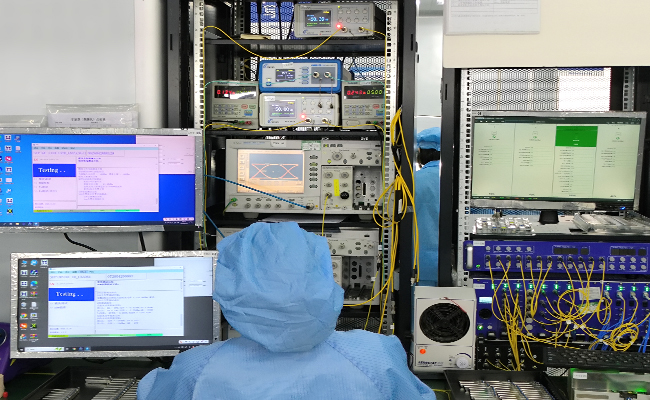
Compatibility Verification

Compatibility validation is available for major switch and router platforms.

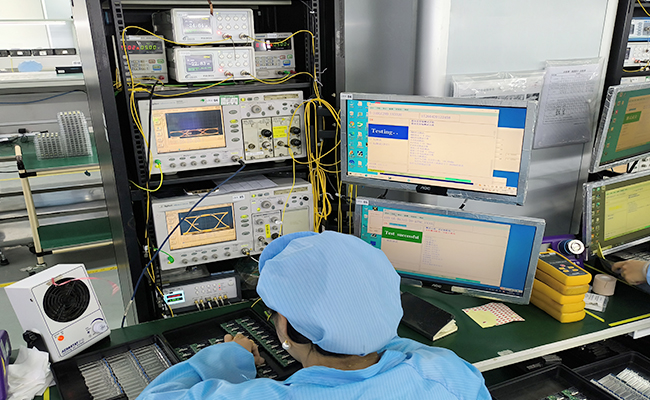
Reliability Screening

Selected products support aging, temperature cycle, and stability testing for demanding applications.

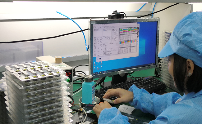
Traceable Quality Control

Inspection and production records support more consistent quality control and batch traceability.

光模块产品详情订购信息---QSFP+